





TL;DR
- This blog is for engineering freshers, university students, and GATE/SSC JE/RRB JE aspirants who want a clear, exam ready understanding of 8051 microcontroller architecture.
- 8051 microcontroller packs a CPU, memory, timers, I/O ports, and a serial port onto a single chip, which is why it remains a common teaching platform for embedded system fundamentals in India.
- This blog breaks down architecture of 8051 microcontroller block by block, its 40 pin layout, and how it processes instructions, backed by a labelled architecture diagram and a worked numerical example.
- You will see where 8051 architecture fits into Indian engineering education, legacy industrial systems, and consumer electronics, along with its relevance to GATE, SSC JE, and RRB JE.
- By the end, you will be able to draw and explain 8051 microcontroller architecture confidently in interviews, labs, and competitive exams.
8051 microcontroller is an 8 bit microcontroller originally introduced by Intel in 1980. It uses a modified Harvard architecture, with separate program and data memory spaces, and 8051 compatible devices are still manufactured by several semiconductor vendors today. What makes 8051 microcontroller architecture worth learning in 2026 is not that chip is cutting edge; it is that architecture of 8051 microcontroller is simple enough to fully understand in a semester while still covering every concept a modern microcontroller architecture builds on: registers, memory organization, timers, interrupts, and I/O.
This guide walks through architecture of 8051 section by section, with a labelled block diagram, explains its 40 pin configuration, and connects each concept to real applications and exam preparation for Indian engineering students.
Also read,
- Swinburne Test of DC Machine: Procedure & Working
- Ward Leonard Method of Speed Control: Working Principle, Advantages and Disadvantages
- Three Phase AC Voltage Controller Waveforms: Modes & Working
What Is an 8051 Microcontroller?
A microcontroller is a small computer with its main components packaged into a single chip. It contains a processor, which runs instructions; memory, which stores instructions and the data they operate on; and input/output (I/O) pins, which connect it to the outside world, such as buttons, motors, sensors, and displays. A microcomputer, on the other hand, usually requires additional memory and peripheral chips to be useful. The 8051 microcontroller combines the processor, memory, and peripherals into a single-chip design, making 8051 microcontrollers relatively inexpensive, compact, and easy to design around.
The 8051’s instruction set and register model are relatively easy to explain and teach, so there is less additional complexity to distract from the fundamental concepts of microcontroller architecture. Once you understand how the 8051 fetches, decodes, and executes an instruction, you can apply the same basic mental model to other microcontroller families, such as AVR, PIC, and ARM Cortex-M.
8051 Microcontroller Architecture: Major Blocks
The 8051 microcontroller architecture consists of several major blocks that work together to execute instructions and control external devices. This section explains the key blocks of the 8051, including the CPU, program and data memory, I/O ports, timers and counters, serial communication unit, interrupt controller, oscillator, and bus system. Understanding these blocks helps engineering students and exam aspirants understand how the 8051 processes data, communicates with peripherals, and performs control operations
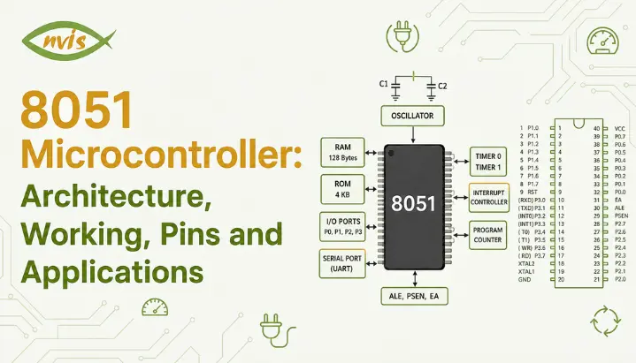
The major blocks of 8051 architecture are connected to each other and with the external world as shown below.
The building blocks in this 8051 microcontroller architecture diagram are:
CPU. processing core. It fetches instructions from program memory, decodes what each one means, and executes them in sequence. It contains an Arithmetic Logic Unit (ALU) for addition, subtraction, and logical comparisons, and an accumulator (register A), which holds the result of most operations.
Program memory and data memory. Two physically and logically separate memory spaces, which is a defining trait of 8051’s modified Harvard architecture. The original 8051 has 4 KB of on chip program ROM and 128 bytes of internal RAM, with room to extend both externally up to 64 KB each.
I/O ports. Four 8-bit ports (P0, P1, P2, and P3), providing 32 port pins in total. Depending on the device and configuration, these pins can be used for general-purpose I/O or alternate functions such as serial communication, interrupts, timers, and external memory interfacing.
Timers and counters. Two 16 bit timers (Timer 0 and Timer 1) that generate precise delays or count external events, such as pulses from a conveyor belt sensor.
Serial port. A full duplex UART style serial interface, with TXD and RXD lines on P3.1 and P3.0, used for serial data transmission and reception.
Interrupt control. A system that lets the CPU pause its current task and respond immediately to an external or internal event, such as a button press, instead of continuously polling for it in a loop.
These blocks do not work in isolation. The CPU fetches instructions from program memory, accesses data from RAM and SFRs, and communicates with peripherals through the 8051’s internal bus structure. Interrupts can temporarily redirect CPU execution to an interrupt service routine when an enabled interrupt occurs. Understanding this interaction, not just memorizing each block separately, is what the architecture of an 8051 microcontroller actually tests in interviews and exams.
CPU: Decision Making Core
8051 microcontroller architecture is essentially an 8 bit CPU with a modified Harvard architecture, with program memory and data memory having different 16 bit address spaces as opposed to a conventional Von Neumann design where both program and data memory are shared into a single address space. Each 16 bit address space can address 64 KB, so the CPU can address 64 KB of external data memory and 64 KB of program memory.
The major blocks of 8051 architecture are connected to each other and with the external world as shown below.
Memory Organization in 8051 Architecture
Program memory stores the instructions executed by the CPU. In the original 8051, this memory is implemented as 4 KB of on-chip ROM, which is non-volatile. The architecture also supports external program memory, allowing up to 64 KB of program-memory address space.
Data memory: The original 8051 has 128 bytes of internal RAM. Its lower 128-byte RAM is organized into three functional areas: 00H–1FH contains four register banks, 20H–2FH is bit-addressable RAM, and 30H–7FH provides general-purpose RAM. The Special Function Registers (SFRs) occupy the upper 128-byte region of the 8051’s internal data address space and are used to control peripherals and CPU functions. This 128 byte RAM is separate from the Special Function Registers (SFRs) that control peripherals such as timers and ports.
Worked example (GATE/SSC JE style): How many distinct memory locations can 8051’s 16 bit address bus access?
A 16-bit address contains 2^16 possible combinations, giving 65,536 addressable locations, or 64 KB.
2^16 = 65,536 locations = 64 KB.
This is the exact calculation behind “64 KB program memory” and “64 KB external data memory” figures you will see in every 8051 datasheet, and it is a common way examiners test whether you understand address bus width rather than just memorizing numbers.
Timers and Counters
Timer 0 and Timer 1 are 16-bit timer/counter units, each formed from two 8-bit registers. In timer mode, a timer increments on an internal machine cycle clock; in counter mode, it increments on external pulses applied to its counter input pin, such as counting conveyor belt sensor triggers. When a timer overflows from its maximum value back to zero, it can generate an interrupt, which is a standard way to create precise, non blocking delays.
Timer behaviour is set through two 8 bit registers: TMOD (Timer Mode) selects operating mode, and TCON (Timer Control) starts, stops, and flags timer. available modes configure a timer as a 13 bit timer, a full 16 bit timer/counter, an 8 bit auto reload timer, or, for Timer 0 specifically, as two independent 8 bit timers.
I/O Ports
The four ports, P0 through P3, provide the 8051’s 32 general-purpose I/O lines and serve as its primary interface with external devices. Some port pins also have alternate functions for serial communication, interrupts, timers, and external memory access.
Port 0 does double duty. In a design with no external memory, it can serve as a plain bidirectional I/O port, but it needs external pull up resistors since classic 8051 does not include internal pull ups on this port. When external memory is connected, Port 0 carries lower address byte and data byte, multiplexed onto the same eight pins.
Port 1 has no alternate function in base 8051, which makes it the simplest port for direct I/O such as LEDs and switches. Port 2 works as general I/O or, during external memory access, carries higher order address bytes (A8 to A15). Port 3 carries pin functions that matter most in practice: serial transmit/receive, two external interrupt inputs, and external timer count inputs.
Interrupts
An interrupt lets CPU suspend normal program execution and jump to a dedicated service routine when a specific event occurs, then return to exactly where it left off. classic 8051 supports five interrupt sources: two external interrupts (INT0, INT1), two timer overflow interrupts (from Timer 0 and Timer 1), and one serial port interrupt for completed transmission or reception.
Interrupts matter in microcontroller architecture because they remove the need to continuously poll a pin or flag in a software loop. Instead of checking “has the button been pressed yet?” thousands of times a second, CPU can do other work and react only when an event actually happens.
Pin Diagram and Pin Description of 8051 Microcontroller
8051 microcontroller ships as a 40 pin Dual Inline Package (DIP). Knowing what each pin does is what lets you actually wire a circuit or answer a pin diagram question correctly in an exam.
Pins 1 to 8 form Port 1 (P1.0 to P1.7), a general purpose bidirectional I/O port with no alternate functions, making it the simplest port for connecting LEDs or push buttons.
Pin 9 is RST, reset pin. Applying a HIGH signal to RST for at least two machine cycles, while the oscillator is running, resets the 8051 and initializes its registers and control logic to their defined reset states.
Pins 10 to 17 form Port 3 (P3.0 to P3.7), carrying alternate functions that matter most: P3.0 (RXD) and P3.1 (TXD) handle serial communication, P3.2 (INT0) and P3.3 (INT1) are external interrupt inputs, P3.4 (T0) and P3.5 (T1) are external timer/counter inputs, and P3.6 (WR) and P3.7 (RD) control write and read operations to external memory.
Pins 18 and 19 (XTAL2 and XTAL1) connect to an external crystal oscillator, which generates clock pulses that drive every internal operation.
Pin 20 is GND, ground reference for chip.
Pins 21 to 28 form Port 2 (P2.0 to P2.7), used as general I/O, or as higher order address byte (A8 to A15) when external memory is connected.
Pin 29 is PSEN (Program Store Enable), an active low output that activates specifically when CPU reads from external program memory.
Pin 30 is ALE (Address Latch Enable), which separates multiplexed address and data signals on Port 0 during external memory access.
Pin 31 is EA (External Access), which controls whether the microcontroller uses its internal program memory. When EA is HIGH, the 8051 uses its internal program memory for the addresses covered by that memory and external program memory beyond that range. When EA is LOW, program code is fetched entirely from external program memory. When EA is low, the CPU fetches program code entirely from external program memory.
Pins 32 to 39 form Port 0 (P0.0 to P0.7), used as general I/O in small designs or as multiplexed lower order address/data bus (AD0 to AD7) when external memory is connected. Port 0 has no internal pull up resistors, so external pull ups are required if you want to use it as a plain output port.
Pin 40 is VCC, supplying +5V that powers the chip.
How 8051 Microcontroller Works: Instruction Execution Cycle
8051 processes every instruction through a repeating fetch decode execution cycle. First, the CPU fetches an instruction from program memory using Program Counter (PC), a register that always holds the address of the next instruction to read. Second, it decodes that instruction, determining whether it is an addition, a data move, a jump, or another operation. Third, it executes instructions, which might update the accumulator, change a PSW flag, or toggle an I/O pin.
This cycle repeats continuously, driven by an external crystal oscillator connected at pins 18 and 19. classic 8051 uses 12 oscillator periods per machine cycle, so a 12 MHz crystal gives a 1 μs machine cycle. Individual instructions take one or more machine cycles depending on their complexity, which is why instruction execution time is not a single fixed number across the instruction set.
8051 vs 8052 vs 8031: Knowing Family
Students often mix up these three names, so here is a plain difference. 8051 is the standard version with 4 KB of internal ROM and 128 bytes of RAM. 8052 is an upgraded version with double ROM (8 KB), double RAM (256 bytes), and a third timer, useful for slightly larger programs. 8031 is an 8051 family device with no on chip program ROM at all, so it must run entirely from external program memory.
Feature | 8051 | 8052 | 8031 |
|---|---|---|---|
Internal ROM | 4 KB | 8 KB | None (external only) |
Internal RAM | 128 bytes | 256 bytes | 128 bytes |
Timers | 2 (16 bit) | 3 (16 bit) | 2 (16 bit) |
Interrupt sources | 5 | 6 | 5 |
Typical use case | General teaching and small embedded designs | Slightly larger programs needing more memory | Designs already using external memory |
Where 8051 Microcontroller Is Used in India
Even with 32 bit microcontrollers dominating new product design, 8051 microcontroller still has a real footprint in Indian industry and education, largely because so much existing equipment, teaching infrastructure, and legacy code runs on it.
In industry, 8051 based controllers have historically handled simple relay control, instrumentation, and small automation tasks. Newer microcontrollers are generally preferred for new industrial designs today, but understanding 8051 microcontroller architecture still matters for engineers who maintain or troubleshoot older control boards, since specific implementations vary by plant and system.
In consumer electronics, appliances like washing machines, microwave ovens, and remote controls historically ran on 8051 variants, and 8051 class devices remain a viable choice for simple, cost sensitive designs where product’s requirements do not demand more processing power.
In automotive systems, 8051 family devices have historically appeared in simpler control and instrumentation circuits, though modern automotive development has largely shifted to ARM based microcontrollers and platforms like AUTOSAR as vehicle electronics have grown more complex.
In engineering education, 8051 is still widely used as an introductory platform because its architecture and instruction set are relatively straightforward to teach. It also introduces students to core concepts such as memory organization, timers, interrupts, and I/O before they move to more advanced microcontroller families.
Exam Relevance: GATE, SSC JE, and RRB JE
For GATE EC, 2026 syllabus does not list 8051 as a dedicated topic. Focus instead on broader concepts it teaches: machine instructions, addressing modes, ALU design, datapath and control unit, and embedded systems fundamentals generally. Treat 8051-specific memorization as supporting preparation for broader computer-organization concepts covered in the official GATE syllabus, rather than as a dedicated GATE topic.
For SSC JE and RRB JE, 8051 related questions may appear depending on specific recruitment notification and applicable syllabus, so check the latest official notification before assuming it is guaranteed. Where it does appear, expect questions on pin functions, timer overflow calculations, and comparisons between Harvard and Von Neumann architecture using 8051 as reference example.
In technical interviews for electronics and embedded systems roles, questions on 8051 microcontroller architecture, such as memory organization, timer configuration, and interrupt handling, are often used to check whether a candidate genuinely understands embedded systems or has only memorized definitions.
Conclusion
8051 microcontroller architecture is decades old, but it remains one of clearest ways to learn how a microcontroller actually works, from CPU and memory organization to timers, I/O ports, interrupts, and instruction execution cycle. You now know how its 40 pins are organized, how its modified Harvard architecture separates program and data memory, and where this chip still shows up in Indian industry and exams today.
The best next step is hands-on practice. Pick up an 8051 development board, write a simple LED blinking program using Timer 0, and watch concepts from this blog play out on real hardware. If you are preparing for SSC JE, RRB JE, or a PSU interview, revisit the pin diagram and architecture block diagram until you can redraw both from memory.
FAQs
8051 microcontroller architecture is based on a modified Harvard architecture, meaning program memory and data memory occupy separate address spaces instead of sharing one memory like a Von Neumann design. This separation is the defining trait of the architecture of 8051 microcontrollers.
The architecture of the 8051 microcontroller is based on a modified Harvard architecture, meaning program memory and data memory occupy separate address spaces, which is a defining characteristic of the 8051’s modified Harvard architecture.
The 8051 microcontroller has 40 pins in its standard DIP package. Thirty two of these form four 8 bit I/O ports (P0 to P3), while the remaining eight handle power, ground, reset, crystal oscillator connections, and control signals for external memory access.
Yes, though mainly for education, legacy system maintenance, and cost-sensitive consumer products rather than new high-performance product design. Many new embedded projects use more capable 32-bit microcontrollers and SoCs, including STM32-family devices and ESP32-family chips, but 8051 architecture remains a commonly used teaching example for introducing microcontroller fundamentals because it clearly demonstrates core concepts every embedded engineer needs.
Yes, mainly for education, legacy system maintenance, and cost sensitive consumer products rather than new high performance designs. Many new embedded projects use more capable 32-bit microcontrollers, including devices from families such as STM32 and ESP32, although the choice depends on application requirements.
A microprocessor, like one in a laptop, contains only CPU and needs external chips for RAM, ROM, and I/O. 8051 microcontroller integrates CPU, RAM, ROM, I/O ports, timers, and a serial port on a single chip, making it self sufficient for embedded applications.
The standard 8051 has two 16 bit timers, Timer 0 and Timer 1, used for generating precise delays or counting external events. upgraded 8052 variant adds a third timer for applications that need an additional independent timing source.