

• Nvis Technology
  • Nvis Technology
  • Nvis Technology
  • Nvis Technology
  • Nvis Technology
  • Nvis Technology
Nvis Technology

Head Office

141-A, Electronic complex, Pardesipura,Indore - 452010 India

Phone: +91 73899 00887 , +91 98932 70303

Email:info@nvistech.com

Request a Quote

Looking for a quality and affordable builder for your next project?


    Nvis Technology

    Toll Free

    +91 73899 00887

    We are happy to meet you during our working hours. Please make an appointment.

    • Monday-Saturday: 9:00 AM - 5:30 PM (IST)
    • Sunday: Closed

    How Does a Shift Register Work? SISO, PISO, SIPO and Universal Types Explained

    TL;DR

    1. This blog is for engineering and diploma students, GATE ECE/EE aspirants, and RRB JE Electronics candidates who need a clear, exam ready understanding of shift registers and how each type moves data.
    2. A shift register is a chain of flip flops that stores and moves binary data one bit position per clock pulse, and its behavior is fixed by how data enters and leaves the chain.
    3. The common SISO, SIPO, PISO and PIPO classifications describe how data enters and leaves a register: serially, in parallel, or a combination of both.
    4. A universal shift register such as the 74194/74HC194 combines serial shifting in both directions, parallel loading, and hold operation on one chip using mode-select inputs, which is why it shows up repeatedly in GATE and RRB JE digital electronics questions.
    5. Shift registers are not a theoretical topic. They run inside SPI communication, LED matrix drivers, UART transmitters, and I/O expander chips used in real embedded designs.
    A shift register is a digital circuit built from a chain of flip flops connected so that output of one stage feeds input of next. On every active clock edge, stored bits move one position along the chain, either toward output or, in bidirectional designs, back toward input. This single behavior, shifting binary data through a register on each clock pulse, is what separates a shift register from ordinary combinational logic and from a simple parallel load register.Shift registers matter because most digital systems need to convert data between serial and parallel form at some point. A microcontroller’s UART sends bits out one at a time over a wire, but the CPU inside works on 8 or 16 bits at once. SIPO shift-register structures provide the basic serial-to-parallel data movement used in many digital and communication interfaces. The same principle scales up to SPI buses, LED matrix drivers, and memory mapped I/O expanders, which is why shift registers appear early in every digital electronics syllabus and stay relevant well into embedded systems design.This article covers how a shift register is built from flip flops, four basic modes (SISO, SIPO, PISO, PIPO), how a universal shift register combines them using mode control logic, a worked timing example, real applications, and where topic shows up in GATE and RRB JE exams.

    Also Read,

    What You Need to Know Before Shift Registers

    A shift register is built entirely from flip flops, so understanding it starts with understanding what a flip flop does. A flip flop is a one bit memory element that captures value present at its input on a clock edge and holds that value steady until the next active edge arrives. D flip flop is type almost universally used inside shift registers, because it copies whatever logic level is on its D input to its Q output moment clock transitions from low to high (or high to low, depending on design).A register, in general, is simply a group of flip flops that share a common clock line and store multiple bits together, the same way a byte in memory stores eight bits as one unit. A shift register is a special case of a register where flip flops are wired in series rather than in parallel: Q output of first flip flop connects to D input of second, second’s Q connects to third’s D, and so on down the chain. Because every flip flop in the chain shares the same clock, all of them update simultaneously on each clock edge, and the effect is that the entire bit pattern appears to slide one position to right (or left) every clock cycle.

    How Data Moves Through a Shift Register

    Consider a 4 bit shift register made of flip flops FF0, FF1, FF2 and FF3, connected so FF0’s output feeds FF1’s input, FF1’s feeds FF2’s, and FF2’s feeds FF3’s. A new bit is applied to FF0’s input just before each clock edge. When the clock ticks, FF0 captures a new bit, FF1 captures what FF0 held a moment ago, FF2 captures what FF1 held, and FF3 captures what FF2 held. bit that was sitting in FF3 is pushed out of the register entirely.This is a mechanical action every shift register performs, regardless of type. What changes between SISO, SIPO, PISO, PIPO and universal shift registers is only the answer to two questions: how does data get into the register, and how is data read back out. Data can enter or exit either serially, meaning one bit is presented per clock pulse through a single line, or in parallel, meaning all bits are presented or read simultaneously through separate lines connected to every flip flop at once.

    Serial In Serial Out (SISO)

    A SISO shift register accepts one bit at a time on its serial input and, after bits have propagated through the full chain, releases them one at a time from the final flip flop’s output. No parallel access to intermediate stages is provided. An n-bit SISO register requires n clock edges for an input bit to propagate through all n stages, making it useful as a digital delay element. For a 4-bit register, the exact timing convention used to describe the delay should be stated when calculating latency.

    Serial In Parallel Out (SIPO)

    A SIPO shift register also accepts data serially, one bit per clock pulse on a single input line, but every flip flop’s Q output is brought out to its own pin. After n clock pulses have loaded n bits into an n bit register, all n bits are available simultaneously on parallel outputs. This is the exact configuration used to convert a serial bitstream, such as data arriving over a single wire from a sensor or a communication bus, into a parallel word a microcontroller or logic circuit can read in one step. widely used 74HC164 and 74HC595 families are built around this principle, with 74HC595 adding an output latch so parallel outputs update only when commanded, keeping the shifting process invisible to whatever is reading outputs.

    Parallel In Serial Out (PISO)

    A PISO shift register does the reverse of SIPO. All n bits are loaded into register simultaneously through n separate parallel input lines, typically during a load pulse, and are then shifted out one bit at a time through a single serial output line over following n clock pulses. Because each flip flop needs to select between two possible next inputs, either parallel data bit during load or previous stage’s output during shifting, PISO registers use a multiplexer in front of every flip flop, controlled by a shared load/shift control line. 74HC165 is a common PISO IC, and this configuration is a standard way to read several parallel switch or sensor inputs using only one data line back to a controller, This approach allows a controller to read multiple parallel inputs using a small number of interface lines.

    Parallel In Parallel Out (PIPO)

    PIPO is often included alongside SISO, SIPO, and PISO when classifying register data-transfer modes. However, a PIPO register does not perform serial shifting; it loads and reads all bits in parallel and is better viewed as a parallel register or storage register. It loads all n bits in parallel and makes them available on parallel outputs, so it behaves more like a parallel storage or buffer register. Strictly speaking, a PIPO configuration does not shift data through a chain the way other three types do; it behaves as a straightforward parallel buffer or temporary storage register, and it is included in the shift register family because the same flip flop chain hardware can be wired to support this mode alongside others.

    Universal Shift Register

    A universal shift register is a single IC that supports serial and parallel data operations, including shift-right, shift-left, hold, and parallel-load modes, with shifting in both directions, and switches between them using dedicated mode select inputs rather than requiring separate circuits for each function. 74194 (and its faster CMOS version, 74HC194) is standard textbook and lab example, and its internal structure illustrates exactly why a universal shift register needs more than just a chain of flip flops.Each flip-flop stage in the 74194 is preceded by selection logic that chooses the appropriate next value from the parallel input, the neighboring stage, the appropriate serial input, or its current state. The S1 and S0 mode-select inputs determine whether the register holds its current value, shifts right, shifts left, or loads data in parallel. Internally, selection logic before each flip-flop chooses the appropriate next input for the selected mode. The S1 and S0 inputs determine whether the register holds, shifts left, shifts right, or parallel-loads, or its own current output (to hold its value unchanged). Two mode select inputs, commonly labelled S1 and S0, control which of these four choices every multiplexer in chip makes simultaneously, so same hardware behaves as a hold register, a right shifting SIPO/SISO register, a left shifting register, or a PIPO parallel load register depending on what logic levels are placed on S1 and S0.
    S1S0Operating mode
    00Hold (no change, data retained)
    01Shift right, serial data entered through DSR
    10Shift left, serial data entered through DSL
    11Parallel load, data D0 to D3 loaded into Q0 to Q3
    74194 also includes an asynchronous active low master reset (MR) pin that forces all outputs low immediately, independent of clock, and separate serial inputs for right shift (DSR) and left shift (DSL) operation. All mode changes and data entry are synchronous, meaning they only take effect on rising edge of clock input, except for master reset. This mode select architecture is the reason a single universal shift register IC can replace what would otherwise require several dedicated SISO, SIPO, PISO and PIPO circuits built from discrete flip flops.

    Worked Example Tracing Data Through a 4 Bit Shift Register

    A short numerical trace makes shifting action concrete and mirrors the style of question asked in GATE and RRB JE digital electronics papers. Consider a 4 bit register with outputs Q0 Q1 Q2 Q3, initially holding 1 0 1 0, configured to shift right on every clock pulse (data advances from Q0 toward Q3) with a serial input DSR that supplies 0, 1, 1, 0 on four successive clock pulses. On each pulse, a new serial bit enters at Q0, every stored bit moves one place toward Q3, and the bit that was in Q3 is shifted out and lost.Before any clock pulse: Q0 Q1 Q2 Q3 = 1 0 1 0.After clock pulse 1 (DSR = 0): bit in Q3 (which was 0) shifts out, every remaining bit moves one place toward Q3, and new serial bit 0 enters at Q0. register now reads 0 1 0 1.After clock pulse 2 (DSR = 1): bit in Q3 (1) shifts out, register content shifts right, and 1 enters at Q0. register now reads 1 0 1 0.After clock pulse 3 (DSR = 1): following the same rule, register becomes 1 1 0 1.After clock pulse 4 (DSR = 0): register becomes 0 1 1 0.This trace shows two things that exam questions routinely test. First, bit shifted out of Q3 is genuinely lost unless it is captured externally, since a simple shift register has no feedback path of its own. Second, after exactly n = 4 clock pulses in a 4 bit register, every original bit has been shifted completely out, which is basis for calculating how many clock pulses a SISO or PISO register needs to fully load or unload a known bit pattern, a calculation that appears directly in past GATE ECE and GATE EE sequential circuits questions.

    Applications of Shift Registers in Real Circuits

    Shift registers are not confined to textbook diagrams. SIPO registers such as 74HC595 devices are commonly used to expand digital outputs for applications such as seven-segment displays, LED indicators, and some LED-matrix designs, allowing a microcontroller to send data serially while controlling multiple parallel outputs because parallel outputs can drive many LEDs while microcontroller only has to send data serially. PISO registers such as the 74HC165 can read a bank of parallel switches or sensor lines and send their states to a controller over a serial connection. Similar serial interfaces are also used in some input-expansion designs.The Serial Peripheral Interface (SPI) protocol used throughout embedded systems is itself built on shift register behavior: at hardware level, both master and slave devices contain internal shift registers, and each clock pulse simultaneously shifts a bit out of one device and into another. A UART transmitter typically uses shift-register-based serialisation to convert parallel transmit data into a serial bitstream, along with timing and framing logic for start and stop bits on the transmit line, A UART receiver uses serial sampling, timing, framing, and shift-register-based data collection to reassemble incoming bits into parallel data. Shift registers also form the basis of ring counters and Johnson counters, sequential circuits built by feeding a shift register’s output back to its own input, which are used for generating timing sequences and simple state machines in control circuits.

    Learning Shift Registers Hands On

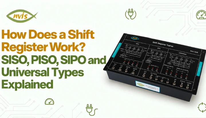
    Reading a function table explains what a universal shift register should do, but watching mode select logic switch between hold, shift left, shift right and parallel load behavior on real hardware is what makes the concept stick for lab exams and viva questions. A dedicated trainer board that lets a student wire and test all four basic shift register types on one platform, such as Shift Registers Trainer, removes guesswork of breadboard wiring errors and lets LED indicators show bit pattern moving through register on every clock pulse, which is a faster way to internalize shifting action than working through timing diagrams alone.

    Shift Registers in GATE, RRB JE and Technical Exams

    Shift registers are explicitly listed under Digital Electronics in the GATE 2026 Instrumentation Engineering syllabus. For GATE EC, sequential circuits are included in the syllabus, but the EC syllabus wording should be checked before stating that “shift registers” are explicitly named. They  are also relevant to the sequential-logic portion of GATE EE’s digital electronics coverage, and Shift-register concepts have been tested in GATE digital/sequential-circuit questions, including questions involving timing, shifting and bit patterns including numerical questions that ask how many clock pulses are needed for a given register to return to its original state. This is distinct from older GATE ECE syllabus coverage of microprocessors. In the current GATE 2026 EC syllabus, shift registers remain explicitly listed under Sequential Circuits, while Computer Organization covers topics such as machine instructions, ALU, datapaths, and control units.For RRB JE, Electronics and Communication and Electronics and Telecommunication streams list Digital Electronics explicitly as a technical ability topic in CBT 2 syllabus, and Digital Electronics is included in the technical syllabus, covering combinational and sequential logic circuits, counters, memories and related topics; shift registers can be studied as part of sequential-logic preparation. SSC JE coverage depends on the engineering discipline and the applicable recruitment notification. Candidates should check the current official syllabus rather than assuming that shift registers are a separately listed topic, so candidates preparing specifically for SSC JE Electrical should weight their preparation time accordingly, while SSC JE Electronics candidates and Shift-register fundamentals can also be relevant in technical interviews for electronics, embedded-systems and digital-design roles.

    Where Shift Register Knowledge Applies on Job

    Shift registers sit inside digital design, embedded systems and VLSI roles far more often than most students expect, since any system that talks over SPI, drives an LED matrix, or expands GPIO pins is very likely using shift register logic internally. Sequential digital circuits can be relevant preparation topics for electronics-focused technical interviews, particularly for roles involving digital systems, embedded systems, or electronics design for junior engineer and trainee roles, and a solid grasp of how SISO, SIPO, PISO, PIPO and universal shift registers behave is exactly kind of fundamental that separates a rehearsed answer from a genuine understanding during those interviews.

    Comparing Shift Register Types

    TypeData inputData outputClock pulses to load/read n bitsTypical ICCommon use
    SISOSerialSerialn74HC164 (wired serial out)Timing delay element
    SIPOSerialParalleln74HC164, 74HC595Serial to parallel conversion, LED/display drivers
    PISOParallelSerialn74HC165Parallel to serial conversion, input expanders
    PIPOParallelParallel1Generic parallel registersTemporary data storage/buffering
    UniversalSerial or parallelSerial or parallelDepends on mode selected74194 / 74HC194Bidirectional shifting, parallel loading, and flexible data movement; shifting can also be used in some binary arithmetic operations.

    Conclusion

    A shift register is fundamentally a chain of flip flops that moves stored bits one position on every clock pulse, and the basic SISO, SIPO, PISO and PIPO classifications describe how data enters and leaves the register, while universal shift registers add selectable operating modes such as shifting, holding, and parallel loading SISO registers use serial input and serial output and can be used for serial data delay, while PISO registers accept parallel data and shift it out serially for parallel-to-serial conversion, SIPO handles serial to parallel conversion for driving displays and reading serial data streams, PIPO acts as a simple parallel buffer, and universal shift register, exemplified by 74194/74HC194, combines all these behaviors using mode select inputs so a single chip can be reconfigured for whichever function a design needs. These circuits are not an isolated exam topic; they run inside SPI communication, UART data framing, LED matrix drivers and GPIO expanders in real embedded hardware, which is why concept keeps showing up from GATE sequential circuits questions through to PSU technical interviews. Building and testing all four types on a lab trainer, then working through a few bit pattern tracing problems by hand, is the most direct way to move from recognizing a function table to being able to design with it.

    Frequently Asked Questions

    What is the main difference between a shift register and a normal register?

    A normal parallel register loads and reads all its bits simultaneously and does not move data between its flip flops. A shift register is specifically wired so that data moves one flip flop position along a chain on every clock pulse, which is what allows it to convert between serial and parallel data formats.

    A PISO register must choose, on every clock edge, between loading a new parallel bit during load phase and shifting in previous stage’s output during shift phase, and a multiplexer in front of each flip flop makes that selection. A basic SIPO register only ever shifts data in from serial input, so no such selection is needed at each stage.

    Exactly 8 clock pulses, since each pulse loads one new serial bit into the first flip flop and shifts existing bits one position further down the 8 bit chain. parallel outputs only reflect a complete 8 bit word once all 8 bits have been clocked in.

    74194 is a universal shift register: its two mode select inputs (S1, S0) let it operate as a hold register, a right shift register, a left shift register, or a parallel load register, all on the same chip, instead of being hardwired to only one of those behaviors.

    Yes. Shift registers are explicitly included under Sequential Circuits in the GATE 2026 ECE syllabus. They are also relevant to sequential-logic coverage in other GATE papers where digital electronics is part of the syllabus, which is separate from microprocessor and computer organization topics that GATE ECE dropped in 2022. Sequential circuit questions involving shift registers continue to appear in GATE papers.

    Shift registers operate inside SPI communication hardware, UART transmitters and receivers, LED matrix and seven segment display drivers such as 74HC595, and parallel-input shift registers such as the 74HC165, which can be used to expand the number of digital inputs available to a microcontroller, making them a routine part of embedded systems and digital hardware design rather than a purely theoretical topic.

    Tags: Shift Register

    How Do Half and Full Subtractors Work? Circuit, Truth Table and Equations

    TL;DR

    1. The purpose of this article is to help engineering and diploma level candidates such as those preparing for GATE, SSC JE and RRB JE exams by providing them an easy-to-understand explanation about half-subtraction problems and their solutions rather than merely memorizing formulas from textbooks.
    2. The half subtractor performs single-bit subtraction using two inputs, A and B, without a borrow-in. The full subtractor takes three inputs A, B, and borrow-in to perform single-bit subtraction while accounting for a borrow from the previous bit position. Full subtractors can be chained to perform multi-bit subtraction.
    3. XOR, AND, OR AND NOT gates are used to build both of these circuits; A full subtractor can also be built by connecting two half-subtractors with an additional OR gate.
    4. The difference output is D = A ⊕ B ⊕ Bin, while the borrow-out equation is Bout = A’B + A’Bin + BBin.
    5. In many modern processor designs, subtraction is implemented using the same adder hardware by adding the 2’s complement of the subtrahend rather than using a completely separate subtractor chain.

    Subtractors are combinational circuits for performing binary subtraction through logic gate operations. There are two types of digital circuits used by computers – an half-subtractor that subtracts two individual binary digits at once, and a full-subtractor where it subtracts two bits but takes into account any borrows received during its operation.

    Binary subtraction is used for comparison, decrementing or computing differences between numbers by an ALU within processor architecture as well as simple calculators. Digital electronics students often encounter half-subtractor and full-subtractor problems at some point during their studies; these come up shortly after learning half-adder and full adder units since they both have similar designs that are commonly tested on tests papers or laboratory assignments.

    The article explains the basics of binary subtraction, including how to derive truth tables, Boolean expressions, and gate-level circuits for half and full subtractors, how we derive truth table values through logic gates operation, how boolean expressions come out of these operations, and finally about designing circuitry at the gate level. Also it includes an example of working multi-bit subtraction which shows how such circuitry is implemented on chips rather than being available as separate components for use by microprocessors.

    Also Read,

    What Do You Need to Know Before Learning Subtractors?

    The subtractive circuit is based on knowledge about binary digits, borrowing during subtraction operations, and simple logic gate circuits. A brief overview of each would be useful to read about before going into detail on circuitry itself.

    Binary subtraction is performed similarly to decimal subtraction by processing each digit individually starting from LSB then MSB. If a smaller value is subtracted by another bigger value then we need to borrow from an adjacent digit like how you do when doing decimal subtraction. For instance, subtracting 1 from 0 in a single binary column isn’t possible without borrowing; hence it would be written as 1 with a borrow of 1 taken from the next column.

    The borrowing process explains why there are two types of subtraction circuitry. The half-subtractor produces an output value but does not receive any input values since its purpose is just to generate a borrow at the least significant position during subtraction when no borrowing occurs beforehand. A full subtractor can receive a borrow from the previous bit position and may generate a new borrow for the next higher bit. It’s similar to this as there are similarities between a half-adder and an adder; so if you’re familiar with them then it’ll be easier for you to understand subtraction circuits from those sources of knowledge.

    The gates involved are same basic building blocks used throughout combinational logic design: The gates involved are basic building blocks used throughout combinational logic: an XOR gate produces 1 when its inputs differ, an AND gate produces 1 only when both inputs are 1, an OR gate produces 1 when at least one input is 1, and a NOT gate inverts its input. These gates are the basic building blocks used to implement half and full subtractor circuits.

    How Does a Half Subtractor Work?

    A half subtractor is a combinational circuit that subtracts one single bit binary number (B, subtrahend) from another (A, minuend) and produces two outputs: Difference (D) and Borrow (Bo). It has exactly two inputs and no borrow in, which is what makes it a “half” circuit rather than a full one.

    The operation being performed is A − B, where A and B are each a single bit. There are four possible input combinations, and working through each one by hand builds the truth table directly.

    When A = 0 and B = 0, subtraction is 0 − 0, giving a difference of 0 with no borrow needed. When A = 0 and B = 1, subtraction is 0 − 1, which cannot be done directly in a single bit; a borrow is taken from the next higher bit, and the difference becomes 1 with borrow = 1. When A = 1 and B = 0, subtraction is 1 − 0, giving a difference of 1 with no borrow. When A = 1 and B = 1, subtraction is 1 − 1, giving a difference of 0 with no borrow.

    Half Subtractor Truth Table

    ABDifference (D)Borrow (Bo)
    0000
    0111
    1010
    1100

    Reading the Difference column against inputs, D is 1 exactly when A and B differ, which is the definition of XOR operation. Reading the Borrow column, Bo is 1 only in a single row where A = 0 and B = 1, which corresponds to A being 0 while B is 1, written as A’ AND B.

    Half Subtractor Equations

    Difference: D = A ⊕ B

    Borrow: Bo = A’B

    These two expressions are already in their simplest form; no further Boolean simplification (through Karnaugh maps or otherwise) is needed, since each expression covers exactly one product term or a single XOR relationship.

    How Do You Build a Half Subtractor Circuit?

    The gate level circuit follows directly from two equations. Difference output needs a single two input XOR gate, fed by A and B. Borrow output needs A to be inverted first (using a NOT gate) and then ANDed with B, so this branch uses one NOT gate and one two input AND gate.

    In total, a half subtractor requires one XOR gate, one AND gate and one NOT gate, three gates in all, with A and B feeding both branches in parallel. Both outputs are produced directly from inputs with no intermediate feedback, which is what makes this a combinational circuit rather than a sequential one: outputs depend only on present input values, not on any stored state.

    Why Do You Need a Full Subtractor?

    A half subtractor works fine for a single bit, but real subtraction problems involve multi bit numbers, and every column after least significant bit may need to account for a borrow taken by the column before it. A half subtractor has no input for that incoming borrow, so it cannot be reused directly for second, third or any higher order bit of a multi bit subtraction.

    A full subtractor solves this by adding a third input, Borrow in (Bin), alongside A and B. It produces the same two outputs as before, Difference (D) and Borrow out (Bout), but now both outputs are calculated using all three inputs. This is exactly the same problem a full adder solves for addition, where a Carry in input lets adder stages be chained together for multi bit arithmetic.

    How Does a Full Subtractor Work?

    With three inputs, a full subtractor truth table has eight rows instead of four. Each row represents subtraction A − B − Bin performed as a single bit operation, with the result expressed as a difference bit and a borrow out bit.

    Full Subtractor Truth Table

    ABBinDifference (D)Borrow out (Bout)
    00000
    00111
    01011
    01101
    10010
    10100
    11000
    11111

    Each row can be checked by working through A − B − Bin directly. For instance, in the second row, A = 0, B = 0 and Bin = 1, so operation is 0 − 0 − 1, which needs a borrow, giving D = 1 and Bout = 1. In the fourth row, A = 0, B = 1 and Bin = 1, so the operation is 0 − 1 − 1. The result requires a borrow, giving a difference bit of 0 and a borrow-out of 1.

    Full Subtractor Equations

    Difference output follows same three variable XOR pattern seen in a full adder’s sum output:

    D = A ⊕ B ⊕ Bin

    Borrow out output is derived by grouping truth table rows where Bout = 1 (rows 2, 3, 4 and 8) using a Karnaugh map. simplified result is:

    Bout = A’B + A’Bin + BBin

    This expression can be read as: a borrow is generated if A is 0 and B is 1 (a direct borrow, same as half subtractor case), or if A is 0 and a borrow already came in, or if B and Bin are both 1 (meaning subtrahend and incoming borrow together exceed what A alone can supply). Each term corresponds to one physical reason a borrow becomes necessary at that bit position.

    How Do You Build a Full Subtractor Using Two Half Subtractors?

    A full subtractor can be built either directly from its two equations using individual gates, or, more commonly in textbooks and lab exercises, by combining two half subtractors with one additional OR gate. Both approaches produce the same truth table; the two half subtractor version is worth understanding because it shows how a complex combinational circuit can be built from a simpler, already understood building block, a pattern that repeats throughout digital design.

    construction works in three steps. First, A and B are fed into first half subtractor, producing an intermediate difference (A ⊕ B) and an intermediate borrow (A’B). Second, this intermediate difference and Bin are fed into a second half subtractor, producing final Difference output (A ⊕ B ⊕ Bin, matching equation derived earlier) and a second intermediate borrow, which is (A ⊕ B)’Bin. Third, two intermediate borrow outputs, from first and second half subtractors, are combined with an OR gate to produce final Bout.

    It is worth confirming that this construction actually reproduces the Bout equation derived earlier from Karnaugh map. Expanding (A ⊕ B)’Bin and OR ing it with A’B algebraically simplifies to A’B + A’Bin + BBin, same expression obtained directly from truth table. This confirms both derivation paths agree, which is a useful check to perform by hand when studying this circuit for an exam, since it builds confidence in Boolean simplification rather than relying on memorized results.

    A full subtractor can be implemented with seven basic gates using the simplified equations: two XOR gates, three AND gates, one NOT gate and one OR gate. Using two standard half-subtractor blocks plus an OR gate also results in seven gates when the gates inside each half subtractor are counted.

    Worked Example: Subtracting Two 4 Bit Binary Numbers

    A single full subtractor handles one bit. Multi bit subtraction is done by chaining full subtractors together, with Borrow out of each stage connected to Borrow in the next higher stage, and least significant stage typically implemented as a half subtractor (or a full subtractor with Bin permanently tied to 0).

    Consider subtracting B = 0110 (decimal 6) from A = 1011 (decimal 11), a calculation in style commonly seen in GATE and SSC JE digital electronics questions.

    Bit 0 (LSB): A0 = 1, B0 = 0, Bin = 0 (no incoming borrow at first stage). D0 = 1 ⊕ 0 ⊕ 0 = 1. Bout0 = A0’B0 + A0’Bin + B0·Bin = 0 + 0 + 0 = 0.

    Bit 1: A1 = 1, B1 = 1, Bin = Bout0 = 0. D1 = 1 ⊕ 1 ⊕ 0 = 0. Bout1 = A1’B1 + A1’Bin + B1·Bin = 0 + 0 + 0 = 0.

    Bit 2: A2 = 0, B2 = 1, Bin = Bout1 = 0. D2 = 0 ⊕ 1 ⊕ 0 = 1. Bout2 = A2’B2 + A2’Bin + B2·Bin = (1)(1) + (1)(0) + (1)(0) = 1.

    Bit 3 (MSB): A3 = 1, B3 = 0, Bin = Bout2 = 1. D3 = 1 ⊕ 0 ⊕ 1 = 0. Bout3 = A3’B3 + A3’Bin + B3·Bin = 0 + 0 + 0 = 0.

    Reading different bits from MSB to LSB gives D3 D2 D1 D0 = 0101, which is decimal 5. This matches the expected result directly: 11 − 6 = 5. final Bout3 = 0 confirms that no borrow was needed beyond the most significant bit, which is expected since A (11) is larger than B (6) and subtraction does not go negative.

    If A had been smaller than B, final borrow out would come out as 1, signaling that true result is negative and that difference bits represent 2’s complement of actual magnitude, a detail that matters when interpreting subtractor output in signed number systems.

    Half Subtractor vs Full Subtractor: What’s Difference?

    AspectHalf SubtractorFull Subtractor
    Inputs2 (A, B)3 (A, B, Bin)
    Outputs2 (D, Bo)2 (D, Bout)
    Borrow in handlingNot acceptedAccepted and used in both outputs
    Difference equationA ⊕ BA ⊕ B ⊕ Bin
    Borrow equationA’BA’B + A’Bin + BBin
    Gate count (direct implementation)3 (XOR, AND, NOT)5 (2 XOR, 2 AND, 1 OR) or 7 using two half subtractors
    Used forLSB of a multi bit subtraction onlyEvery bit position after LSB
    CascadableNoYes

    Where Are Subtractors Used in Real Circuits?

    Subtractor circuits form part of the arithmetic logic unit (ALU) inside a processor block responsible for arithmetic and logic operations on binary data. Subtractor logic explains the hardware principles behind binary subtraction, while practical ALUs often implement subtraction using an adder and 2’s complement arithmetic whenever a program executes a subtraction instruction, compares two values, or decrements a counter or memory address.

    Beyond processors, subtraction logic can also be used in some comparison circuits, calculators, and other digital systems that need to determine numerical differences, and in any digital system that needs to compute a numerical difference directly in hardware rather than through software.

    Are Subtractors Actually Used in Practice, or Just Adders with 2’s Complement?

    This is a genuine design question, and answer matters for anyone studying computer organization alongside digital logic. Most modern ALUs do not implement a separate chain of full subtractor circuits at all. Instead, they reuse the same adder hardware for both addition and subtraction by representing negative numbers in 2’s complement form. Subtracting B from A is computed as A + (B’s 2’s complement), which is B inverted bit by bit (1’s complement) with 1 added to the result. A full adder chain, already present in ALU for addition, then performs this operation without any dedicated subtractor gates.

    This approach is preferred in real hardware because it avoids duplicating arithmetic circuitry. Building both a full adder chain and a full subtractor chain would roughly double gate count needed for basic arithmetic, while 2’s complement method lets a single adder circuit, combined with some inverters and a control signal, perform both operations.

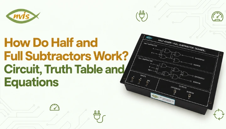
    This does not make half and full subtractor circuits covered in this article irrelevant. They remain standard way subtraction is taught in digital electronics courses because they build Boolean design skills directly, from truth table to equation to gate level circuit, and they appear frequently as standalone circuits in lab experiments, viva questions and competitive exams, even when production hardware favors adder based approach. Lab trainers such as Nvis 6554 Adders and Subtractors trainers are built specifically around this dedicated circuit approach, letting students patch together half and full subtractor stages by hand and observe truth table behavior directly on hardware rather than only in simulation.

    Half and Full Subtractors in Exams: GATE, SSC JE and RRB JE

    Half and full subtractors fall under combinational logic circuits, a core topic in the Digital Logic section of GATE syllabus for Computer Science, Electronics and Communication, and Electrical Engineering papers. Questions typically test truth table derivation, Boolean simplification of borrow output using Karnaugh maps, and gate count comparisons between different implementations of the same circuit, exactly the kind of derivation worked through in this article.

    For SSC JE and RRB JE, digital electronics topics may be tested through objective questions covering concepts such as logic gates, Boolean algebra, and combinational circuits. Questions on these topics can involve truth tables, Boolean expressions, logic-gate implementations, and circuit diagrams. Practicing the derivation of these results can help candidates handle questions that require more than recalling the final equations.

    Digital logic fundamentals may also be relevant in technical selection processes for engineering roles at organisations such as BEL, BHEL, ISRO and Power Grid, depending on the role and recruitment process.

    Conclusion

    Half and full subtractors are combinational circuits built entirely from XOR, AND, OR and NOT gates, and the difference between them comes down to one input: borrow in. A half subtractor handles a single bit with no incoming borrow, producing D = A ⊕ B and Bo = A’B. A full subtractor adds Bin input so multi bit subtraction can be chained bit by bit, producing D = A ⊕ B ⊕ Bin and Bout = A’B + A’Bin + BBin, and it can be built directly from two half subtractors plus one OR gate.

    Working through truth table derivation by hand, confirming Boolean equations against it, and tracing a multi bit example like one worked through above builds a kind of understanding that holds up in a lab viva or a GATE style question, not just on a memorized diagram. For hands-on practice with actual gate level behavior of these circuits, a digital electronics trainer such as Nvis 6554 lets students patch together half and full subtractor stages and verify each truth table row directly on hardware.

    FAQs

    What is the main difference between a half subtractor and a full subtractor?

    A half subtractor has two inputs (A and B) and does not accept a borrow in, so it can only be used for the least significant bit of a subtraction. A full subtractor has three inputs (A, B and Bin), which lets it be chained with other full subtractors to perform multi bit binary subtraction.

    Difference output is D = A ⊕ B ⊕ Bin. The output, after Karnaugh map simplification, is Bout = A’B + A’Bin + BBin.

    Yes. First half subtractor processes A and B, second half subtractor processes first one’s difference output along with Bin, and an OR gate combines two intermediate borrow outputs to produce final Bout.

    A half subtractor needs three gates: one XOR, one AND and one NOT. A full subtractor can be implemented using seven basic gates from the simplified Boolean equations, or seven gates using two half subtractors and an OR gate.

    Yes. They fall under combinational logic circuits in Digital Logic syllabus for GATE (CS, ECE and EE papers) and are a standard topic in SSC JE and RRB JE Electronics and Electrical papers, often tested through truth table and circuit diagram questions rather than pure recall.

    Yes. They fall under combinational logic circuits in Digital Logic syllabus for GATE (CS, ECE and EE papers) and are a standard topic in SSC JE and RRB JE Electronics and Electrical papers, often tested through truth table and circuit diagram questions rather than pure recall.

    Tags: Half Subtractor and Full Subtractor

    Which Digital Electronics Projects Are Best for Engineering Students?

    TL;DR

    1. This blog is for electronics, electrical, and instrumentation engineering students (and diploma students) who need digital electronics project ideas that actually build exam relevant and interview relevant skills, not just a list of buzzword titles.
    2. Most “digital electronics project ideas” lists online are either 100+ item link dumps with no technical depth or two line project abstracts that don’t explain what project actually teaches.
    3. This guide organizes 15 projects by difficulty tier (combinational logic, sequential logic, and microcontroller integrated systems), explains working principle and components behind each one, and walks through a full worked design example.
    4. A digital electronics project is only useful if you can explain its truth table, state diagram, or timing behavior in a viva or interview; picking a project for its title without understanding its logic defeats the purpose.
    5. Pick a project one level above your current comfort zone, build it on a trainer kit or breadboard before touching code, and be ready to justify every IC and every logical decision you made.
    Digital electronics project ideas commonly include circuits built from digital logic building blocks such as gates, flip flops, counters, registers, and multiplexers. More advanced projects can also combine these fundamentals with microcontrollers and embedded software. For engineering students in electronics, electrical, instrumentation, and computer science branches, these projects serve three purposes at once: they satisfy academic project requirements, they reinforce concepts that are relevant to exams such as GATE and RRB JE, while also giving interviewers a concrete project that students can explain during technical discussions.Difficulty with most digital electronics project resources is not a shortage of ideas. A search for “digital electronics project ideas” returns lists running into hundreds, but the vast majority describe a project in one or two sentences and move on. That format works for browsing but fails the moment a student sits down to build, or worse, sits in front of an interview panel and cannot explain what their own circuit does. This guide takes a narrower set of projects and goes deeper on each: logic being demonstrated, components involved, and why the project is worth building in the first place.Projects below are grouped into three tiers, combinational logic projects for students starting out, sequential logic projects for those comfortable with basic gates, and microcontroller integrated projects for students ready to combine digital logic with embedded programming. A full worked design example and a section on lab tools follow the project list.

    Also Read,

    What Fundamentals Should a Digital Electronics Project Actually Test?

    Before picking a project, it helps to be clear on what digital electronics as a subject is actually built from, since every project on this list is really just an application of a small number of core ideas.Digital electronics deals with circuits that process information using discrete logic states, commonly represented as logic 0 and logic 1 and associated with defined voltage ranges. This is different from analog electronics, where a signal can take any value across a continuous range. One advantage of digital logic is that receivers interpret signals within defined voltage ranges as logic states, allowing some noise margin without changing the interpreted value.At the logic level, digital circuits can be represented using combinations of logic gates such as AND, OR, NOT, NAND, NOR, XOR, and XNOR, with Boolean algebra providing the mathematical framework for describing their behavior. Circuits are classified into two categories that matter for choosing a project. A combinational circuit produces an output that depends only on current input values, with no memory of past inputs; adders, multiplexers, and decoders fall into this category. A sequential circuit produces an output that depends on both current inputs and circuit’s past state, which requires memory elements called flip flops; counters, registers, and finite state machines fall here.This distinction is the reason the project list below is split into combinational and sequential tiers. Combinational circuits are simpler to design, debug, and explain, since there is no timing or clock behavior to reason about. Sequential circuits add complexity of clocking, state transitions, and timing diagrams, which is exactly why they represent the next skill level up.

    How to Choose a Digital Electronics Project Based on Your Skill Level

    A project is worth building only if it stretches you slightly beyond what you already know how to design. A student who has only wired basic logic gates should not jump straight into a microcontroller based digital voltmeter, and a student already comfortable with counters and shift registers gets little out of building yet another logic gate demonstration.The beginner tier below assumes familiarity with Boolean algebra and basic gate ICs (74 series family such as 7400, 7408, 7432, and 7486) and no prior exposure to sequential circuits. The intermediate tier assumes comfort with flip flops (7474, 7476) and requires understanding of clock signals and state transitions. Advanced tier assumes both of the above plus basic microcontroller programming, typically on an 8051, AVR, or Arduino platform, since several practical digital systems today combine hardwired logic with software controlled logic for flexibility.Two other decisions shape which project fits: whether you build on a breadboard with discrete ICs or use a digital IC trainer kit with a built in power supply, ZIF sockets, and I/O indicators, and whether final submission needs to be a standalone hardware circuit or can include a microcontroller based implementation. Academic evaluators generally reward projects that make underlying logic visible, so a project built from discrete gate and flip flop ICs, where every connection can be traced and explained, tends to demonstrate stronger fundamentals than the same function implemented as a few lines of microcontroller code.

    Beginner Projects: Combinational Logic Circuits

    These five projects use only logic gates and combinational building blocks. No clock signal or memory element is involved, which keeps debugging straightforward: a wrong output always traces back to a wrong gate connection or an incorrect truth table implementation.

    1. Full Adder and Full Subtractor Circuit

    A full adder is a fundamental building block used in many digital arithmetic circuits, including adders and arithmetic units such as ALUs. It takes three single bit inputs, two operands and a carry in from a previous stage, and produces a sum and a carry out. Building it from individual XOR, AND, and OR gates, rather than using a ready made adder IC, forces you to derive sum and carry expressions from truth table yourself: Sum = A ⊕ B ⊕ Cin, and Carry out = AB + BCin + ACin. A full subtractor follows the same pattern with borrow logic instead of carry logic. Cascading four full adders builds a 4 bit parallel adder, a natural extension that demonstrates how larger arithmetic circuits are built from repeated smaller units.

    2. BCD to Seven Segment Display Decoder

    This project converts a 4 bit binary coded decimal (BCD) input into seven output signals needed to light correct segments of a seven segment display. core learning value is in constructing truth tables and deriving Boolean expressions for each of seven segment outputs, then simplifying them using Karnaugh maps before wiring the circuit. Students frequently first build this project by hand using discrete gates, then rebuild the same function using a dedicated decoder IC such as 7447, which makes the value of using purpose built ICs concrete rather than theoretical.

    3. Multiplexer Based Data Selector

    A multiplexer (MUX) selects one of several input lines and routes it to a single output line, based on the value of select lines. A 4 to 1 MUX project (using an IC such as 74153) demonstrates how select line combinations govern which input reaches output, and is a natural lead in to implementing arbitrary Boolean functions using MUX based logic, a technique that appears directly in GATE level digital circuit design questions.

    4. Priority Encoder for Interrupt Handling

    An encoder converts one of several input lines into a corresponding binary code. A basic encoder assumes that only one input is active at a time, while a priority encoder can handle multiple active inputs by assigning priority to one of them. A priority encoder adds a rule that if multiple inputs are active simultaneously, only the highest priority input’s code is output. This project models exactly how interrupt controllers in real processors decide which of several simultaneous interrupt requests to service first, which makes it a good bridge project between pure digital logic and computer organization concepts.

    5. Digital Magnitude Comparator

    A comparator circuit takes two multi bit binary numbers and determines whether first is greater than, less than, or equal to second, using cascaded XOR and gate logic (implemented in ICs such as 7485). Building a 4 bit comparator and then cascading two of them to compare 8 bit numbers demonstrates the same expandability principle seen in full adder projects, and reinforces how larger digital systems are constructed from smaller repeatable blocks.

    Intermediate Projects: Sequential Logic Circuits

    These five projects introduce flip flops, clocking, and state behavior. Unlike combinational circuits, a working sequential circuit needs correct clock edge triggering (positive edge, negative edge, or level triggering), and debugging often means reading a timing diagram rather than a truth table.

    6. Mod N Synchronous Counter

    A synchronous counter increments its count on every clock pulse, with all flip flops triggered by the same clock signal simultaneously, which avoids propagation delay problems of an asynchronous (ripple) counter. A Mod N counter counts from 0 to N−1 and then resets, rather than counting through the full range available from its flip flops. This is one of most commonly assigned sequential logic projects because designing one from scratch requires working through a state table, deriving flip flop excitation equations, and verifying design against a timing diagram, which is a precisely designed process tested in GATE and PSU technical interviews. A full worked example for designing a Mod 6 counter follows in the next section.

    7. Traffic Light Controller Using Counters and Decoders

    A traffic light controller is a finite state machine (FSM) that cycles through a fixed sequence of states (red, red yellow, green, yellow) with different durations for each state, typically implemented using a counter to track time within each state and a decoder to translate counter’s output into correct combination of LED outputs. This project is popular precisely because it takes an everyday system and reduces it to explicit states and transitions, and it scales naturally: a basic two way intersection can later be extended to a four way intersection with pedestrian signals, which is a common way to differentiate a project during evaluation.

    8. Digital Clock Using Counter ICs

    A digital clock built from counter ICs (typically 7490 decade counters or 74192 up/down counters) rather than a microcontroller demonstrates cascaded counting with modulus conversion: seconds and minutes need Mod 60 counters, while hours need a Mod 12 or Mod 24 counter, each requiring different reset logic. The project can also introduce multiplexed seven-segment display driving. In multiplexing, the digits are switched rapidly one at a time so that they appear continuously lit to the human eye, reducing the number of driver lines required.

    9. Shift Register Based Serial to Parallel Converter

    A shift register stores and shifts binary data one bit at a time on each clock pulse, using cascaded flip flops (commonly 74164 or 74195 IC family). A serial to parallel converter project takes data arriving one bit at a time on a single line and, after the correct number of clock pulses, makes the entire word available on parallel output lines simultaneously. This project demonstrates the shift-register and serial-data concepts used in serial communication systems such as UART and SPI, which makes it a strong bridge into embedded systems and communication engineering topics.

    10. Frequency Divider Circuit

    Each flip flop in a cascaded chain divides input clock frequency by two, since a flip flop toggles its output once for every two clock pulses at its input. A frequency divider project chaining four flip flops to divide a given clock frequency by 16, and displaying or measuring resulting frequency, is a compact project that reinforces both flip flop toggling behavior and frequency domain thinking, which carries over directly into timer and clock management topics in microcontroller based systems.

    Advanced Projects: Microcontroller Integrated Digital Systems

    These five projects combine digital logic concepts with microcontrollers, ADCs, sensors, and embedded programming. They are useful for students who want to extend their digital electronics fundamentals into embedded and practical system design.

    11. Digital Voltmeter Using ADC and Microcontroller

    This project uses an analog to digital converter (ADC0808 or microcontroller’s built in ADC) to sample an analog voltage, converts digital reading into a displayable value, and shows it on a seven segment or LCD display. The core digital electronics concept being tested is resolution: For an ideal 8-bit ADC with a given reference range, the nominal LSB size is approximately the reference range divided by 256. Practical ADC resolution also depends on factors such as quantization, noise, reference accuracy, and ADC architecture. Understanding this resolution limit, and how it changes with a 10 bit or 12 bit ADC, is a concept that shows up repeatedly in both academic exams and instrumentation focused PSU interviews.

    12. Bidirectional Visitor Counter with Automatic Room Light Control

    This project uses two IR sensor pairs positioned to detect direction of movement (whether a person entered or exited a room) and drives an up/down counter accordingly, while also switching room lighting on or off automatically based on whether count is greater than zero. direction sensing logic, determining which of two sensors is triggered first, is a genuinely instructive part of this project, since it requires a small state machine of its own to disambiguate entry from exit reliably.

    13. Digital Code Lock Using Flip Flops or Microcontroller

    A digital code lock accepts a sequence of button presses and only unlocks (activates a relay or LED) if the sequence matches a pre-set combination in correct order. A flip flop based implementation uses a sequence of D flip flops, each enabling next only if the previous stage matched correctly, which is a clean demonstration of sequential logic used for a genuinely practical purpose. A microcontroller based version replaces flip flop chains with a stored sequence compared in software, which is worth building alongside hardware versions specifically to compare two design approaches to the same problem.

    14. Elevator Controller Using a Finite State Machine

    An elevator controller project models an elevator’s behavior (idle, moving up, moving down, door open) as an explicit finite state machine, with transitions triggered by floor call button presses. This project is more demanding than a basic traffic light controller because its state transitions depend on inputs such as floor requests, the elevator’s current position, and its current operating state rather than following one fixed sequence, closer to how a general purpose sequential controller is actually designed in industry. It is a strong final year project specifically because FSM design (state diagram, state table, and next state logic) can be defended in detail during evaluation.

    15. UART Based Digital Communication Module

    Building a basic UART (Universal Asynchronous Receiver Transmitter) transmitter and receiver pair, either from discrete shift registers and timing logic or using a microcontroller’s built in UART peripheral, ties together frequency division (for baud rate generation), shift registers (for serial to parallel and parallel to serial conversion), and start/stop bit framing. Understanding UART at this level of detail is directly useful, since serial communication debugging is a routine task in embedded systems roles across PSUs and private sector electronics companies.

    Worked Example: Designing a Mod 6 Synchronous Counter

    Since a Mod N counter appears repeatedly across the project list above and is also a standard GATE and PSU interview design question, working through the design process end to end is worth doing in full.Problem: Design a Mod 6 synchronous counter using JK flip flops that counts 0, 1, 2, 3, 4, 5, and then resets to 0.Step 1: Determine the number of flip flops needed. A counter needs enough flip flops to represent all required states. With n flip flops, 2ⁿ states are available. Since Mod 6 requires 6 states (000 to 101 in binary), and 2² = 4 is insufficient while 2³ = 8 is sufficient, three flip flops (labeled Q2, Q1, Q0) are required, with states 110 and 111 left unused.Step 2: Write a state transition table. counter cycles through states 000 → 001 → 010 → 011 → 100 → 101 → 000. For each flip flop, note its present state and required next state at every transition.Step 3: Derive JK excitation table for each flip flop. For a JK flip flop, excitation rules are: to hold state 0 → 0, J = 0 and K = don’t care (X); to transition 0 → 1, J = 1 and K = X; to transition 1 → 0, J = X and K = 1; to hold state 1 → 1, J = X and K = 0. Applying these rules to every bit at every transition in the state table produces required J and K inputs for Q0, Q1, and Q2 at each of six states.Step 4: Simplify using Karnaugh maps. Plotting each of six J and K input values (J0, K0, J1, K1, J2, K2) against present states Q2Q1Q0 on separate Karnaugh maps, and grouping resulting 1s and don’t care cells, gives simplified Boolean expressions. One valid simplification, when the unused states 110 and 111 are treated as don’t-care conditions, is J0 = 1, K0 = 1, J1 = Q0, K1 = Q0, J2 = Q1Q0, and K2 = Q0. The resulting circuit produces the required 000 → 001 → 010 → 011 → 100 → 101 → 000 sequence from the valid states. However, because the unused states are treated as don’t-cares, the resulting behavior from 110 and 111 should be checked separately. These equations produce the required sequence 000 → 001 → 010 → 011 → 100 → 101 → 000, though “don’t care” cells for unused states 110 and 111 mean more than one valid simplification exists, and any correct simplification is acceptable as long as it produces required sequence.Step 5: Wire circuit and add reset logic. Connect derived expressions to J and K inputs of three flip flops, all sharing a common clock line for synchronous operation. Because 110 and 111 are unused states, the design should also define how the circuit behaves if it enters either state. A reset or recovery condition can be added to force the counter back to 000, or the unused states can be assigned transitions that return the counter to the valid sequence.This same five step process, determine flip flop count, build state table, derive excitation equations, simplify with Karnaugh maps, and add reset logic, applies to designing any Mod N counter, and understanding it thoroughly is what separates a student who can only wire a pre designed circuit from one who can design a new sequential circuit from a specification.

    Tools You Need to Build These Projects

    A breadboard with jumper wires and individually purchased ICs works for combinational projects, but sequential and microcontroller integrated projects benefit from more structured lab equipment, since debugging a clocked circuit on loose breadboard connections is disproportionately harder than debugging a static combinational circuit.A digital IC trainer kit, such as NV6550 Digital IC Trainer, provides a regulated power supply, ZIF sockets for quick IC insertion without bent pins, and built in input switches and output LED indicators, which removes a significant source of project failures that have nothing to do with underlying digital logic, loose wires, wrong voltage levels, or a bent IC pin, and lets debugging time go toward actual circuit design instead. For projects spanning combinational circuits (adders, decoders, multiplexers), sequential circuits (flip flops, counters, registers), and display interfacing (BCD to seven segment decoding), a trainer kit built specifically around these building blocks covers most of beginner and intermediate project list above on a single piece of lab equipment.For microcontroller integrated tier, an additional development board (an 8051 or AVR trainer kit, or an Arduino board) and a basic understanding of embedded C or Arduino programming are needed alongside digital logic fundamentals, since these projects deliberately combine both skill sets.

    Digital Electronics and Competitive Exam Relevance

    Digital electronics is one of core subjects in GATE Electronics and Communication Engineering (ECE) and Electrical Engineering (EE) syllabi, covering number systems, Boolean algebra and logic gate minimization, combinational circuit design, and sequential circuit design including flip flops, counters, and registers. Students preparing for GATE ECE or EE benefit directly from having actually built combinational and sequential circuits rather than only having studied them on paper, since the digital-circuit topics tested in GATE include combinational and sequential logic, flip-flops, counters, registers, and related design concepts, making the Mod 6 counter a useful practical example of these fundamentals.For SSC JE and RRB JE, the exact treatment of digital electronics depends on the examination and discipline. For example, the current RRB JE Electronics & Allied Engineering syllabus explicitly includes digital electronics topics such as number systems, Boolean algebra, logic gates, combinational and sequential circuits, ADC/DAC, counters, and memories. Students should check the notification for their specific recruitment cycle. That said, Technical interviews for electronics, instrumentation, and embedded roles may ask candidates to explain projects they have built, including their truth tables, timing diagrams, state transitions, or implementation choices, which makes projects on this list relevant for interview preparation even where they are not directly tested in a particular exam’s written syllabus. Candidates should verify the current syllabus on official SSC and RRB notifications before assuming any subject’s exact weightage, since exam patterns are revised periodically.

    Career Pathways Where These Skills Are Used

    Digital electronics fundamentals can be relevant to entry-level roles in electronics, instrumentation, hardware testing, and embedded systems across public-sector and private-sector organisations. The specific skills and eligibility requirements vary by organisation and recruitment cycle. Digital electronics skills can support entry-level opportunities in areas such as hardware testing, embedded systems, electronics design, and instrumentation. Specific roles and eligibility requirements vary by organization and recruitment cycle, so students should check current official job notifications before relying on specific eligibility criteria or recruitment details.In private sector, digital design skills transfer into embedded systems engineer, hardware design engineer, and test engineer roles across electronics manufacturing and semiconductor industries, where ability to read a datasheet, design a state machine, and debug a timing diagram remains a practical, non negotiable skill regardless of how much of actual circuit design has moved into FPGAs and programmable logic in modern products.

    Comparing Three Project Tiers

    AspectBeginner (Combinational)Intermediate (Sequential)Advanced (Microcontroller Integrated)
    Core concept testedBoolean logic, gate level designClocking, state transitions, memoryDigital logic combined with embedded programming
    Typical componentsLogic gate ICs (7400 series), MUX/decoder ICsFlip flop ICs, counter ICs, shift registersMicrocontroller board, ADC, sensors, plus logic ICs
    Debugging methodTruth table verificationTiming diagram analysisCombination of code debugging and hardware timing checks
    Design skill demonstratedBoolean simplification (K maps)State table design, excitation equationsSystem level integration of hardware and software
    Recommended toolBreadboard or digital IC trainer kitDigital IC trainer kit with clock sourceTrainer kit plus microcontroller development board

    Which Digital Electronics Project Should You Actually Build?

    Start with a project from the tier that matches your current comfort with Boolean algebra and gate ICs, not the tier that sounds most impressive on a project report cover page. A well built full adder circuit that you can explain gate by gate demonstrates more engineering understanding to an evaluator or interviewer than a microcontroller based system you copied from a tutorial without following underlying logic. Work through the Mod 6 counter design process on paper for whichever sequential project you choose, since that five-step design method develops the systematic reasoning used in digital-logic exam problems, technical interviews, and hardware design. Build on a proper digital IC trainer kit where possible, since it removes wiring related failures that have nothing to do with your circuit design and lets you focus debugging time on logic itself.

    FAQs

    What is the difference between a digital electronics project and an embedded systems project?

    A digital electronics project focuses on circuits built from logic gates, flip flops, and related ICs, where behavior is fixed by hardware wiring. An embedded systems project uses a microcontroller running software to implement similar or more complex behavior. Several projects on this list, including digital code lock and UART module, can be built either way, which is a useful exercise for understanding trade offs between two approaches.

    No. beginner and intermediate tiers above, covering combinational circuits and sequential circuits like counters and shift registers, use only logic gate and flip flop ICs and require no programming knowledge. Programming becomes necessary only for advanced, microcontroller integrated tier.

    A project with genuine design decisions, such as an elevator controller or traffic light controller, can give you more material to explain during a final-year evaluation, including its state diagram, transition logic, and implementation choices. A finite state machine also gives you a clear design process to explain during your viva, rather than focusing only on the final output.

    Yes. FPGA and programmable logic design still requires understanding the same combinational and sequential logic fundamentals, number systems, Boolean simplification, flip flop behavior, and state machine design, that these discrete IC projects teach. The implementation platform has changed in industry, but underlying digital logic concepts have not.

    Wiring flip flops without accounting for clock edge triggering correctly, mixing positive edge triggered and negative edge triggered ICs in the same circuit, or without a shared clock line across all flip flops in a synchronous design. This produces a circuit that behaves unpredictably even though every individual connection looks correct, which is why understanding timing diagrams matters as much as understanding truth tables.

    GATE ECE and EE test digital electronics through numerical design problems, such as deriving flip flop excitation equations or simplifying Boolean expressions using Karnaugh maps. The exact depth and coverage of digital electronics vary by examination and discipline. For example, the current RRB JE Electronics & Allied Engineering syllabus explicitly includes combinational and sequential logic, counters, ADC/DAC and memories, focusing more on general electrical and basic electronics fundamentals, though underlying knowledge still helps in PSU technical interviews where candidates are asked to explain projects they have built.

    Tags: Digital Electronics

    What Is a Multiplexer and a Demultiplexer? Working, Circuit and Truth Table

    TL;DR

    1. The article is aimed at engineering students, diploma students, and GATE/SSC JE/RRB JE aspirants to have an easy-to-understand explanation about multiplexer and demuxer concepts from their exams.
    2. A multiplexer (MUX) selects one of several input signals and routes the selected signal to a single output. A demultiplexer (DEMUX) performs the reverse operation by routing one input signal to one of several outputs based on the select lines.
    3. The number of data inputs in a MUX or outputs in a DEMUX is determined by 2^n, where n is the number of select lines.
    4. Truth table and Boolean expression of a 2:1, 4:1, and 8:1 multiplexer is given here with some example calculations to show which select line outputs an output.
    5. The multiplexer is a part of GATE ECE combinational circuit course; it also appears as an exam question for MUX and DEMUX questions during SSC JE, RRB JE, and PSU technical interview exams.
    A multiplexer receives multiple inputs and uses select lines to route one selected input to a single output. A demultiplexer performs the reverse operation by routing one input to one of several outputs according to the select-line combination. Multiplexers and demultiplexers are common digital building blocks used in systems such as computers, communication equipment, and processor-based systems, including applications involving bus and signal routing.They are useful because connecting every device directly to every other device would require many physical or logical connections. In digital electronics, a multiplexer is used to solve this issue because it acts like an electronic switch selecting which inputs get through at any particular time whereas a demultiplexer performs the opposite operation by routing one input to one of several outputs.This article explains how multiplexers and demultiplexers work, including their truth tables, Boolean expressions, basic logic-gate implementations, applications, and common exam questions.

    Also Read,

    What You Need to Know Before Multiplexers and Demultiplexers

    A multiplexer is a combinational circuit whose output depends on the current input and select-line values, not on previous states. A demultiplexer is also a combinational circuit, but it routes one input signal to one of several outputs based on the select lines. This is different from sequential circuits such as flip-flops and counters, whose outputs can depend on previous states.There are three basic concepts related to digital circuits that should be understood first. Firstly, binary select lines are available for choosing between two options – 0 and 1. With n select lines, a circuit can distinguish between 2^n unique combinations, and this single relationship governs size of every multiplexer and demultiplexer discussed below. Also secondly, basic logic gates such as AND, OR, and NOT gates are used to construct MUX and DEMUX circuits from within a computer system. Thirdly, an idea about how to distinguish between a data line and a control line; within those systems there are data lines that transmit real-time information whereas selection lines determine whether any particular data line should be activated or not. Two common points of confusion when learning multiplexer truth tables are understanding the select-line combinations and identifying which input is connected to the output.

    What Is a Multiplexer?

    Multiplexers are also known by their acronyms such as “MUX” which refers to an electronic device that combines several input signals into one signal through selection paths based on control lines. Any particular selection of lines will determine which single input is linked to an output while others are not considered at once.A multiplexer has an input count that must be a power of 2 based on how many selection wires there are to it. With n select lines a multiplexer is able to pick out from 2^n signals. This gives a standard family of multiplexer sizes: 2:1 (1 select line, 2 inputs), 4:1 (2 select lines, 4 inputs), 8:1 (3 select lines, 8 inputs), and 16:1 (4 select lines, 16 inputs).Multiplexers are similar to rotary selectors for choosing between multiple channels on an antenna set. Lines are switches; only a selected station’s signal is heard by an individual at that time whereas other stations’ signals stay unheard. The same applies to switching behavior; however, an electronic switch is made up of logic gate circuits instead of physical contacts.

    2:1 Multiplexer: Simplest Case

    A 2:1 multiplexer has two data inputs (I0 and I1), one select line (S), and one output (Y). When S = 0, input I0 passes to output; when S = 1, input I1 passes to output.

    S

    Y
    0I0
    1

    I1

    Boolean expression for a 2:1 multiplexer is:Y = I0·S′ + I1·SHere S′ represents complement (NOT) of S. This expression is built from one NOT gate, two AND gates, and one OR gate: NOT gate generates S′, each AND gate combines one data input with either S or S′, and OR gate combines both AND outputs into the final result. Larger multiplexers can be implemented by combining smaller multiplexers or by using a larger gate-level implementation with additional select lines.

    4:1 Multiplexer

    A 4:1 multiplexer has four data inputs (I0 to I3), two select lines (S1 and S0), and one output (Y). two select lines together produce four unique combinations, each of which activates exactly one input line.

    S1

    S0Y

    0

    0

    I0

    0

    1

    I1

    1

    0

    I2

    11

    I3

    Boolean expression extends 2:1 case:Y = I0·S1′S0′ + I1·S1′S0 + I2·S1S0′ + I3·S1S0Each product term is active for exactly one select line combination, which is why only one input reaches output at a time. Circuit wise, a 4:1 multiplexer needs four 3 input AND gates (one per data line, each combined with appropriate select line values), a 4 input OR gate, and two NOT gates to generate S1′ and S0′.

    8:1 and 16:1 Multiplexers

    An 8:1 multiplexer follows the same pattern with three select lines (S2, S1, S0) selecting among eight inputs (I0 to I7), and its Boolean expression has eight product terms, one for each 3 bit select combination. The 16:1 multiplexer has four select lines and sixteen inputs. Instead of constructing them anew each time, a bigger multiplexer can be built through a combination of several small ones. An 8:1 multiplexer can be constructed using two 4:1 multiplexers followed by one 2:1 multiplexer. The two 4:1 multiplexers share two select lines, while the third select line controls the final 2:1 multiplexer.. Two select lines are applied to both 4:1 multiplexers, while the remaining select line controls the final 2:1 multiplexer. Two select lines are shared by the 4:1 multiplexers, while the third select line controls the 2:1 multiplexer that chooses between their outputs. The same modular design applies to commercial multiplexer ICs as well; this method of implementation is used by engineers when they need an efficient way of performing any kind of logic operation through multiplexers which appear frequently on test papers from universities like GATE level exam questions.

    What Is a Demultiplexer?

    A demultiplexer (DEMUX) performs the reverse data-routing operation of a multiplexer. It has one data input, multiple outputs, and select lines that determine which output receives the input signal. The select-line combination determines which output is selected. In the active-high convention used in this example, the selected output follows the input while the other outputs remain at logic 0.Just like multiplexers, the number of outputs is determined by an 2^n rule according to the number of select lines: a 1:2 demultiplexer requires 1 select line, a 1:4 demultiplexer needs 2, a 1:8 demultiplexer needs 3, and a 1:16 demultiplexer needs 4.A DEMUX can be compared to a railway junction where one incoming route can be directed to one of several outgoing tracks. The select lines act like switching controls that determine the destination based on the selected route. A train is unchanged by switching to another track but it can be redirected towards a different location depending upon that switch setting. Electrically, the input signal remains the same; the select lines simply determine which output receives that signal.

    1:4 Demultiplexer Truth Table

    A 1:4 demultiplexer has one data input (D), two select lines (S1, S0), and four outputs (Y0 to Y3).

    S1

    S0Y0Y1Y2

    Y3

    0

    0D00

    0

    010D0

    0

    1

    000D

    0

    1

    1000

    D

    Boolean expressions for each output follow directly from truth table:Y0 = D·S1′S0′ Y1 = D·S1′S0 Y2 = D·S1S0′ Y3 = D·S1S0Each output is generated by a single AND gate that combines data input with appropriate select line term, exactly mirroring the internal structure of the multiplexer but with AND gates feeding separate outputs instead of a shared OR gate. This structural symmetry is why multiplexers and demultiplexers are usually taught together: once truth table logic for one is clear, the other follows by reversing the direction of data flow.

    Multiplexer and Demultiplexer: How They Work Together

    Multiplexers are often paired with demultiplexers for sharing of a single transmission line between many sources and receivers. On the transmission side, there is a multiplexer which picks out from among the multiplexer, selects one of the inputs and sends it through the shared channel.. At the receiving end, the demultiplexer routes the incoming signal to the appropriate output line based on the select lines.To ensure proper operation, the multiplexer and demultiplexer must use corresponding select-line combinations; therefore, For a simple MUX-DEMUX arrangement, the receiver uses the corresponding select-line combination to route the transmitted signal to the intended output. In a simple MUX-DEMUX arrangement, the transmitter and receiver need coordinated selection or timing information so that the receiver can correctly identify the intended channel. This principle is related to time-division multiplexing (TDM), which allows multiple signals to share a communication channel.

    Worked Example: Implementing a Boolean Function Using a Multiplexer

    A frequently asked question in university exams and competitive papers is to implement a given Boolean function using a multiplexer rather than discrete logic gates. Consider function:F(A, B, C) = Σm(1, 3, 5, 6)This means F = 1 for minterms 1, 3, 5, and 6, and F = 0 for all other combinations of A, B, C.Step 1: Choose multiplexer size. With three variables, an 8:1 multiplexer can implement this function directly, using A, B, and C as three select lines and tying each data input to either 0 or 1 based on the truth table.Step 2: Build the truth table.

    A

    BCMintermF
    000m0

    0

    001m1

    1

    0

    10m20
    011m3

    1

    100m4

    0

    1

    01m51
    110m6

    1

    111m7

    0

    Step 3: Map each minterm to a data input. Using A as S2, B as S1, and C as S0, connect multiplexer’s data inputs directly to F values from table: I0 = 0, I1 = 1, I2 = 0, I3 = 1, I4 = 0, I5 = 1, I6 = 1, I7 = 0.Step 4: Verify. When A = 1, B = 0, C = 1 (minterm 5), select lines S2S1S0 = 101 select input I5, which was set to 1, matching F = 1 from the truth table. same check holds for every row.This method, connecting select lines to function’s input variables and data lines directly to function’s output values, avoids need for separate Karnaugh map minimization and is one of fastest ways to solve multiplexer based logic design questions under exam time pressure.

    Common Multiplexer and Demultiplexer ICs

    In practice, multiplexers and demultiplexers are implemented using multiple logic gates or dedicated ICs. TTL and CMOS logic families include ICs that implement multiplexer, demultiplexer, and related logic functions. 74151 is an 8:1 multiplexer that comes as a single IC package, often found at digital design labs and cited by textbooks due to its simple pin configuration. The 74153 package has two separate 4:1 multiplexers on a single chip for use where there is need of two independent data selection operations at same time. The 74LS138 is primarily a 3-to-8-line decoder with active-low outputs, but it can also be used as a demultiplexer by using one of its enable inputs as the data input while the three address inputs act as select inputs. Because its outputs are active-low, its demultiplexer behavior is inverted compared with the active-high DEMUX example above, which is worth noting because exam questions sometimes test decoder to demultiplexer conversion specifically. The manufacturer datasheet is a reliable source for precise pin configuration details as well as electrical specifications because there may be slight differences among manufacturers’ models and packages.For students who want to verify this behavior physically rather than only on paper, a dedicated multiplexer and demultiplexer trainer kit lets you build and test a 4 to 1 line multiplexer and a 1 to 4 line demultiplexer using onboard SPDT switches for select line control and LED indicators to read output directly, which makes truth table behavior visible rather than something to only memorize.

    Applications of Multiplexers and Demultiplexers

    Multiplexers and demultiplexers are used in communication, computer, and control systems to route or share signals efficiently when multiple data sources need to use limited communication paths.In communication systems, multiplexing techniques such as time-division multiplexing (TDM) allow multiple signals to share a communication channel. A multiplexer is one of the circuit-level building blocks that can be used for signal selection and routing. A multiplexer is an electronic device that can be found inside of computers for selecting among several inputs going towards one output line within its circuitry. A 2^n:1 multiplexer can implement any Boolean function of n variables by using those variables as the select lines and connecting each data input to the corresponding 0 or 1 value from the function’s truth table hence this problem is often asked on exams. In a communication system, a demultiplexing stage can separate a multiplexed stream into its constituent channels or signals. In memory and I/O systems, decoders are commonly used to select specific memory locations or peripheral devices based on address inputs.

    Multiplexer vs Demultiplexer: Quick Comparison

    ParameterMultiplexer (MUX)Demultiplexer (DEMUX)
    Number of inputsMultiple (2^n)Single
    Number of outputsSingleMultiple (2^n)
    FunctionSelects one input, routes to outputRoutes single input to one selected output
    Also known asData selectorData distributor
    Select linesn lines for 2^n inputsn lines for 2^n outputs
    Common IC examples74151, 7415374138 (as decoder/demux)
    Typical useCombining multiple signals onto one lineDistributing one signal to multiple destinations

    Where This Topic Shows Up in Indian Technical Exams

    In the GATE 2026 Electronics and Communication Engineering syllabus, multiplexers are covered under Digital Electronics and combinational logic topics. This makes multiplexers a relevant concept for GATE ECE preparation. Multiplexers remain part of the current GATE 2026 EC Digital Electronics syllabus, since these are core combinational logic topics evaluated separately from microprocessor architecture.Beyond GATE, digital electronics fundamentals including multiplexers and demultiplexers are commonly tested in SSC JE and RRB JE electronics and electrical papers, and the same concepts frequently come up in technical interviews for PSU recruitment in electronics, telecommunication, and instrumentation roles. Candidates preparing for these exams should be comfortable deriving truth tables from scratch, writing Boolean expression for a given multiplexer or demultiplexer size, and solving Boolean function implementation problems of kind worked through earlier in this article, since these tend to appear as both objective and descriptive questions.

    Multiplexer and Demultiplexer: What to Remember

    Multiplexers choose among many inputs for sending them through an output channel whereas demultiplexers take one input signal and route it to one of several output channels based on the select lines; both are controlled via select lines following the 2^n relationship between select line count and data line count. Knowledge of truth tables and Boolean expressions for 2:1 and 4:1 can be used to generalize this concept to 8:1, 16:1, and more complex multiplexers and demultiplexers. They are useful for selecting and distributing signals in digital systems, including communication and computer systems. Their truth tables, Boolean expressions, and logic-function implementation are important concepts for digital-electronics exam preparation. Once you understand these concepts, practice Boolean-function problems before moving on to related topics such as decoders, encoders, and flip-flops. The worked example above provides a good starting point.

    FAQs

    What is the main difference between a multiplexer and a demultiplexer?

    A multiplexer has multiple inputs and one output, selecting one input to pass through based on select lines. A demultiplexer has one input and multiple outputs, routing that single input to one selected output. They perform opposite operations.

    An 8:1 multiplexer needs three select lines, since 2^3 = 8. In general, a multiplexer or demultiplexer with n select lines can handle 2^n data lines.

    Yes. A 2^n:1 multiplexer can implement any Boolean function of n variables by connecting the function’s variables to select lines and function’s truth table output values to data inputs, as shown in the worked example in this article.

    The 74138 is a 3-to-8-line decoder/demultiplexer. With suitable enable connections, one enable input can be used as the data input while the three address inputs act as select inputs. Its outputs are active-low, so its behavior differs from an active-high 1:8 DEMUX truth table.

    Yes. Multiplexers are explicitly listed in the Digital Electronics section of the GATE 2026 Electronics and Communication Engineering syllabus, along with Boolean algebra, Karnaugh maps, and decoders. Demultiplexers are not named separately in syllabus but follow directly from the same combinational logic concepts.

    A mechanical switch requires physical movement to change connections, while a multiplexer changes its output instantly based on electrical logic level applied to its select lines, making it suitable for high speed digital switching where mechanical switches would be far too slow.


    Tags: Multiplexer and Demultiplexer

    How Do You Perform Logic Gate Experiments in a Digital Electronics Lab?

    TL;DR

    1. This blog is for engineering and diploma students, GATE/SSC JE/RRB JE aspirants, and lab instructors who need a clear, accurate procedure for logic gate experiments in a digital electronics lab.
    2. A logic gate experiment verifies a gate’s truth table by applying every input combination on a breadboard mounted IC and observing output through an LED or a multimeter reading.
    3. Common logic gates such as AND, OR, NOT, XOR, and XNOR can be implemented using only NAND gates or only NOR gates because both are universal gates. Realizing basic gates using universal gates is also a common digital-logic laboratory exercise.
    4. Correct results depend on getting three things right: TTL/CMOS voltage levels, IC pin identification, and never leaving an input pin floating.
    5. Logic gate fundamentals are relevant to digital-electronics topics covered in GATE and applicable SSC JE and RRB JE examinations
    A logic gate experiment is a hands-on lab exercise in which a student builds a digital logic circuit using integrated circuits (ICs) on a breadboard and confirms that its output matches gate’s theoretical truth table. In a digital electronics lab, this is usually the first practical exercise students perform, because it connects Boolean algebra taught in class with a physical, measurable circuit.These experiments matter because digital electronics rely heavily on basic logic gates such as AND, OR, NOT, NAND, NOR, XOR, and XNOR. Combinational and sequential circuits are built by combining these and other digital logic elements. Many combinational and sequential circuits, including adders, flip-flops, and counters, are built from combinations of logic gates and other digital building blocks. A student who can wire a gate correctly, read its datasheet, and verify its truth table with confidence has the foundation needed for the rest of a digital logic course.This article walks through what apparatus a logic gate experiment needs, how TTL logic levels decide whether an output reads as HIGH or LOW, exact step by step procedure used to verify a truth table, how NAND and NOR gates are used to build every other gate, precautions that prevent most common wiring mistakes, and where these fundamentals show up in GATE, SSC JE, and RRB JE exams.

    Also Read,

    What Do You Need Before Starting a Logic Gate Experiment?

    A standard logic gate experiment does not require expensive equipment. A basic setup may include a breadboard or digital trainer kit, a regulated power supply appropriate for the IC family, suitable logic ICs, jumper wires, LED indicators with current-limiting resistors, and a digital multimeter. Many labs now use a dedicated IC trainer kit that already has toggle switches for inputs and LED indicators for outputs built into board, which removes the need to wire a separate LED for every test.IC choice depends on which gate is being tested. 7400 series TTL family assigns one IC part number to each gate type: 7404 is a hex inverter (six NOT gates in one package), 7408 is a quad two input AND gate, 7432 is a quad two input OR gate, 7400 is a quad two input NAND gate, 7402 is a quad two input NOR gate, and 7486 is a quad two input XOR gate. The classic 14-pin DIP versions of these ICs commonly use pin 14 for VCC and pin 7 for GND. However, package and pin assignments can vary, so always verify the exact device datasheet. However, always check the specific IC’s datasheet before making connections, as pin arrangements and package types can vary across the 74-series family.Before touching the circuit, a student should have an IC’s pin diagram in hand. Datasheets are freely available from manufacturers such as Texas Instruments and STMicroelectronics, and identifying pins correctly before powering the board avoids the single most common cause of a failed experiment: a reversed or miswired Vcc and ground connection, which can permanently damage IC.It also helps to be fluent in standard logic gate symbols before starting, since circuit diagrams in a lab manual use schematic symbols rather than IC part numbers. AND gate symbol is a D shaped block, OR gate symbol has a curved input edge and a pointed output, NOT gate is a triangle with a small circle (bubble) at output, and NAND and NOR gates use AND and OR symbols respectively with that same output bubble added to indicate inversion. Recognizing these symbols quickly is what lets a student translate a textbook circuit diagram into an actual breadboard layout without re-deriving the truth table from scratch each time.

    How Do TTL Logic Levels Decide a HIGH or LOW Output?

    A logic gate does not read voltage as a simple 0V or 5V signal. TTL (Transistor Transistor Logic) ICs, which power most 7400 series gates, work within defined voltage bands, and understanding these bands is what lets a student correctly interpret a multimeter reading during verification.For standard 5V TTL devices, any input voltage of 2.0V or higher is read as logic HIGH (VIH minimum), and any input voltage of 0.8V or lower is read as logic LOW (VIL maximum). For a standard 5V TTL family, the guaranteed input and output voltage limits depend on the specific IC family and datasheet. For example, 74LS00 specifies VIH(min) = 2.0V and VIL(max) = 0.8V; its output limits should be taken from the relevant datasheet rather than generalized to every 7400-series device. The noise margin is determined from the guaranteed output and input voltage limits. For a specific TTL family, the HIGH-level noise margin is VOH(min) − VIH(min), while the LOW-level noise margin is VIL(max) − VOL(max), the HIGH-level noise margin is calculated as VOH(min) − VIH(min), while the LOW-level noise margin is calculated as VIL(max) − VOL(max). Always use the values specified in the relevant IC datasheet. It exists so that small voltage drops or interference along a wire do not flip a HIGH signal into a LOW one by time it reaches the next gate’s input.
    ParameterStandard TTL (5V)Meaning
    VIH (min)2.0 VMinimum input voltage read as HIGH
    VIL (max)0.8 VMaximum input voltage read as LOW
    VOH (min)2.7 VMinimum guaranteed output voltage for HIGH
    VOL (max)0.4 VMaximum guaranteed output voltage for LOW
    Vcc5 V ± 0.25 VSupply voltage
    This is why a multimeter reading of exactly 5V is not required to confirm a HIGH output. For a specific TTL family, use the datasheet’s guaranteed VOH and VOL limits to interpret the output. For example, an output above the specified VOH(min) is guaranteed HIGH, while an output below VOL(max) is guaranteed LOW. Avoid treating intermediate readings as valid logic states. A voltage in the undefined region should not be interpreted as a valid logic HIGH or LOW. It may result from loading, wiring problems, an improperly driven input, or device-specific behaviour, so the circuit and datasheet should be checked.

    What Is Step by Step Procedure to Verify a Logic Gate’s Truth Table?

    Verifying a truth table is a core practical exercise in every digital electronics lab, and procedure stays largely the same whether the gate under test is a NOT, AND, OR, NAND, NOR, or XOR gate.Step 1: Identify IC and its pinout. Confirm gate type, IC part number, and exact pin numbers for inputs, output, Vcc, and ground before placing IC on breadboard.Step 2: Mount IC on breadboard. Place the IC across the central gap of the breadboard so that its two rows of pins sit in separate strips, which prevents pins from being shorted to each other.Step 3: Power should always be connected last, after every input and output wire is in place, and switched off before making any change to circuit.Step 4: Wire inputs. Connect gate’s input pins to toggle switches or jumper wires that can be manually set to +5V (logic 1) or ground (logic 0). Never leave an input pin unconnected. A floating TTL input may often be interpreted as HIGH, but it is not a recommended way to define a logic state and can be susceptible to noise or unintended behavior. Do not rely on a floating input; define the required logic level using the appropriate circuit connection.Step 5: Wire output. Connect the gate output to an LED and suitable current-limiting resistor only according to the trainer kit’s wiring scheme and the IC’s output-current limits. For TTL ICs, follow the recommended current direction and loading conditions in the datasheet or lab manual.Step 6: Apply each input combination. Starting from the truth table for that gate, apply every possible combination of 0s and 1s to inputs, one at a time. For a two input gate, this means four combinations: 00, 01, 10, and 11.Step 7: Record output for each combination. Note the LED indicator state according to the trainer kit’s wiring. Do not assume that an illuminated LED always represents logic 1. Alternatively, use the measured output voltage and the IC’s datasheet limits to determine whether the output is HIGH or LOW.Step 8: Compare against the theoretical truth table. Match observed output pattern against gate’s known truth table. A matching output pattern across all input combinations indicates that the IC and circuit are behaving as expected under the test conditions.Running both LED method and multimeter method on the same IC is good practice, because it separates a wiring mistake from a genuine component fault. If LED behaves correctly but voltage reading looks marginal, IC itself is usually fine and fault lies in connection.

    How Do You Realize All Basic Gates Using Only NAND or NOR Gates?

    NAND and NOR are called universal gates because either one, used on its own, can reproduce behavior of every other logic gate, including AND, OR, and NOT. This property follows directly from De Morgan’s theorems, and it is one of most frequently assigned practical exercises after basic truth table verification.To build a NOT gate from a NAND gate, both inputs of NAND are tied together and driven by the same signal. Since NAND(A, A) = (AA)’ = A’, this reproduces inversion exactly. To build an AND gate from NAND gates, a NAND gate’s output is fed into a NAND based NOT gate, since AND is simply NAND followed by inversion. To build an OR gate from NAND gates, each input is first inverted using a NAND based NOT gate, and two inverted signals are then fed into a third NAND gate; this works because of De Morgan’s law, which states that A + B = (A’B’)’.The same logic applies to NOR gates in reverse. A NOR gate with its inputs tied together produces a NOT gate. An OR gate is built from a NOR gate followed by a NOR based inverter. An AND gate is built by inverting both inputs first and then feeding them into a NOR gate, since AB = (A’ + B’)’.Worked example: Consider Boolean expression Y = AB + BC’, Consider the Boolean function Y = AB + BC’. The following example shows how it can be implemented using only NAND gates. Realizing this using only NAND gates follows these steps:
    1. Generate C’ using a NAND based NOT gate (tie both inputs of a NAND gate to C).
    2. Generate AB using a NAND gate followed by a NAND based NOT gate (since AND = NAND + NOT).
    3. Generate BC’ same way, using a NAND gate followed by a NAND based NOT gate.
    4. Combine AB and BC’ using NAND based OR gate construction described above (invert both terms, then NAND them together).
    Lab trainers built specifically for this exercise make wiring faster and less error prone than a bare breadboard setup. Nvis 6552 Universal Gates NAND & NOR Trainer, for instance, uses patch cord connections to let students construct NOT, AND, and OR gates from NAND and NOR gates without wiring a fresh breadboard circuit for every configuration, which is useful when a lab session needs to cover all six standard reconstructions in a single sitting.

    What Precautions Should You Follow During a Logic Gate Experiment?

    Most failed logic gate experiments trace back to a small number of avoidable mistakes. Checking IC orientation before power up is the first line of defense, since ICs have a notch or dot marking pin 1, and inserting one backward routes Vcc and ground to wrong pins.Power should always be connected last, after every input and output wire is in place, and switched off before making any change to circuit. This prevents momentary short circuits from damaging IC while wires are being moved. Do not leave required inputs floating. For unused inputs, follow the specific IC family’s datasheet or lab-manual recommendation for connecting them to an appropriate defined logic level for connecting them to an appropriate logic level. Follow the specific IC family’s datasheet or lab-manual recommendation for tying unused inputs to an appropriate logic level, since a floating input can pick up noise and produce unpredictable output states.Current limiting resistors are required for every LED in circuit, since TTL outputs are not designed to drive an LED directly without one, and doing so risks exceeding IC’s maximum output current rating. Finally, a multimeter should be used to confirm Vcc and ground before applying power for the first time on any new circuit, since this check can catch wiring errors before power is applied.

    Where Are Logic Gates Applied Beyond Lab?

    gates tested in a lab experiment are the same building blocks used in real digital systems. NAND and NOR gates are important universal building blocks in digital logic. They can be used to implement other logic functions, although modern ICs and processors are not necessarily manufactured using only one type of gate. Combinational circuits built from these gates form adders, multiplexers, and encoders, while Sequential circuits use logic gates together with storage elements to implement structures such as registers and counters, which are used as building blocks in embedded systems, digital communication equipment, and control systems.

    Comparing TTL and CMOS Gate Families

    Digital electronics labs typically stock more than one IC logic family, and choice affects both experiment’s power requirements and its voltage behavior.
    Feature74xx (Standard TTL)74LSxx (Low Power Schottky TTL)74HCxx (High Speed CMOS)
    Supply voltage5V5V2V–6V
    Typical propagation delay~10 ns~9 10 ns~8 10 ns
    Power consumptionHigherLower than standard TTLLowest, especially at rest
    Noise immunityModerateModerateHigher
    Common lab useLegacy trainersMost common in current labsMixed voltage and low power circuits
    74LS-series ICs are commonly used in digital electronics training and laboratory setups because they operate from a 5V supply and provide TTL-compatible input characteristics. Actual IC availability varies by institution and laboratory.

    Why Are Logic Gate Experiments Important for GATE, SSC JE, and RRB JE Aspirants?

    Digital logic is an important area within the relevant technical syllabi for several engineering examinations in India. GATE syllabus for Electronics and Communication Engineering (EC) and Electrical Engineering (EE) explicitly lists Boolean algebra, logic gates, minimization of Boolean functions, and combinational and sequential circuits under Digital Circuits sectio, where digital and combinational logic topics form part of the syllabus. Questions can involve Boolean logic, logic circuits, and related circuit analysis.SSC JE and RRB JE technical papers for Electronics and Electrical branches Depending on the post and examination syllabus, questions may cover truth tables, Boolean simplification, logic gates, and universal-gate implementation, since these exams draw heavily from standard diploma and degree level digital electronics syllabi. Logic gates and digital electronics are relevant to the technical syllabi used for several engineering and railway examinations. However, the number and frequency of questions can vary from one examination and year to another, which makes lab experiments described in this article directly relevant to exam preparation and not just a classroom formality.

    Conclusion

    Logic gate experiments verify the theoretical truth table of a gate against real circuit behavior, using an IC mounted on a breadboard, correctly identified pins, and either LED- or multimeter-based output verification. The exercise depends on understanding TTL voltage thresholds, following a consistent step by step wiring procedure, and applying precautions such as never leaving an input floating. NAND and NOR gates deserve particular attention because their universal property, ability to build every other gate from just one of them, is both a core lab exercise and a recurring question type in GATE, SSC JE, and RRB JE technical papers. Students preparing for these exams should treat lab bench and question paper as the same skill practiced twice: get wiring right on breadboard, and Boolean algebra behind it becomes far easier to apply on paper.

    FAQs

    What is the difference between a logic gate experiment and a truth table?

    A truth table is a theoretical list of every possible output for a given set of inputs. A logic gate experiment is the practical exercise of building an actual circuit and confirming that its measured output matches that theoretical table for every input combination.

    NAND and NOR are called universal gates because either one, on its own, can be used to construct every other basic logic gate, including AND, OR, and NOT, through input combinations described by De Morgan’s theorems.

    A floating TTL input is not a reliable way to define a logic level. Although a standard TTL input may often behave as HIGH when left open, a floating TTL input is not a reliable way to define a logic level. Although an open TTL input may often behave as HIGH, it can be affected by noise and should not be relied upon. Connect inputs to a defined logic level according to the IC manufacturer’s datasheet or the laboratory’s recommended wiring method to an appropriate defined logic level according to the manufacturer’s datasheet or the laboratory’s recommended wiring method.

    Yes. Simulation tools such as CircuitVerse, Multisim, and Logisim let students build and test the same gate circuits virtually, which is useful for practicing circuit design before or alongside hands on lab sessions, though hands on wiring remains part of most college lab evaluations.

    Digital logic, including Boolean algebra, logic gate behavior, and universal gate realization, is a listed topic in GATE ECE/EE syllabus andDigital logic concepts may also be relevant to SSC JE and RRB JE technical examinations depending on the applicable post and syllabus.

    Confirm Vcc and ground connections with a multimeter before powering the circuit, then verify output against the known truth table using both an LED indicator and a multimeter voltage reading, since agreement between the two methods provides additional evidence that the circuit and IC are behaving as expected.

    Tags: Logic Gate Experiment

    What Are Logic Gates? Symbols, Truth Tables and Types Explained

    TL;DR

    1. The article is aimed at engineering and diploma students, as well as GATE, SSC JE, and RRB JE candidates who want an easy-to-understand explanation of logic gates and digital circuits.
    2. A logic gate is an electronic circuit that implements a Boolean function by converting one or more binary inputs into a single binary output according to predefined logic rules.
    3. Seven common types of logic gates AND, OR, NOT, NAND, NOR, XOR, and XNOR have their own symbols, truth tables, and Boolean expressions.
    4. Both NAND and NOR are known as universal gates because each can be used to construct the other basic logic gates and, therefore, any Boolean function. This concept is commonly tested in digital electronics exams.
    5. Logic gates are essential building blocks of digital circuits, including calculator arithmetic units, processors, and satellite onboard computers. They are used to build both combinational and sequential circuits.
    A logic gate is a basic building block of digital electronics. It accepts one or more binary inputs and produces a binary output according to a defined logical rule. In practical circuits, gates are implemented using electronic components such as transistors and are combined to build larger digital systems.Logic gates are important in electronic devices for much more than just textbook concepts. Digital circuit design is an important part for GATE ECE, EE and IN exams while also appearing on SSC JE and RRB JE technical papers too. VLSI engineers and embedded systems developers use digital logic concepts when designing circuits, writing RTL code, and working with programmable or integrated digital systems.This article explains logic gate definitions, symbols, truth tables, and Boolean expressions. It also explains why NAND and NOR are called universal gates, with examples relevant to digital electronics exams.

    Also Read,

    What Do You Need to Know Before Logic Gates?

    Logic gates rest on two ideas: binary representation and Boolean algebra.Digital circuits use two logic states, usually represented as LOW and HIGH. These states correspond to voltage ranges rather than two exact voltage values. For standard TTL inputs, voltages up to about 0.8 V are generally recognized as LOW, while voltages above about 2 V are recognized as HIGH. CMOS logic levels depend on the specific device and its supply voltage. All signals within an electronic device are represented by numbers, characters, and command codes which can be expressed through sequences of bits.The Boolean algebra was invented by George Boole as an algebraic system for describing combinations of two-valued variables. Boolean algebra defines three basic operations: AND, represented by logical multiplication; OR, represented by logical addition; and NOT, which represents complementation. Logic gates are just an implementation by means of electronics for some type of Boolean operation (or combinations thereof). After understanding those concepts clearly, it would be easy to understand how each gate works by following their truth tables properly.

    What Is a Logic Gate?

    A logic gate is a digital circuit with one or more binary inputs and exactly one binary output, where output depends entirely on the current combination of inputs according to a defined logic function. Internally, gates are built from transistors (in modern ICs, almost always MOSFETs in CMOS technology), but at design level, engineers work with the gate as an abstract logic block rather than its internal transistor circuit.Each gate is described using three equivalent representations that appear constantly in coursework and exams: logic symbol, used in circuit diagrams; truth table, which lists output for every possible input combination; and Boolean expression, which states the same relationship algebraically. Being able to move between these three representations is an important skill in digital electronics.

    Types of Logic Gates With Symbols, Truth Tables, and Boolean Expressions

    The seven commonly discussed logic gates are AND, OR, NOT, NAND, NOR, XOR, and XNOR. AND, OR, and NOT are the basic gates, while NAND and NOR are universal gates. XOR and XNOR are commonly used in arithmetic, comparison, and other digital logic applications.

    AND Gate

    AND gate produces a HIGH output only when all of its inputs are HIGH. Its Boolean expression is Y = A·B for a two input gate, and it is represented in circuit diagrams by a D shaped symbol with a flat input side. A common TTL implementation is the 7408, which contains four 2-input AND gates.
    ABY = A·B
    000
    010
    100
    111
    AND gate behaves the way word “and” does in everyday language: a condition is true only when every requirement is met together. A safety interlock circuit that must confirm both a door is closed and a machine guard is in place before allowing a motor to start is a direct real world instance of AND logic.

    OR Gate

    OR gate produces a HIGH output when at least one input is HIGH. Its Boolean expression is Y = A + B, and its symbol has a curved input side that tapers to a point at output. A common TTL part is IC 7432, a quad 2 input OR gate.
    ABY = A+B
    000
    011
    101
    111
    OR logic matches situations where any one of several conditions is sufficient to trigger an action, such as a fire alarm circuit that should sound if a smoke sensor or a heat sensor detects a hazard, since either input alone should activate the alarm.

    NOT Gate

    A NOT gate, also called an inverter, is only a gate with a single input. It inverts its input: a 0 becomes 1, and a 1 becomes 0. Its Boolean expression is written as Y = A’ or Y = Ā, and its symbol is a triangle followed by a small circle (bubble) at output, where bubble specifically denotes inversion. IC 7404 is a hex inverter, packing six independent NOT gates in one chip.
    AY = A’
    01
    10
    The inversion bubble is worth remembering carefully, because the same bubble symbol appears on the output of NAND and NOR gates, and confusing where it is placed is one of most common mistakes in exam diagrams.

    NAND Gate

    A NAND gate can be considered as an AND gate followed by another NOT gate. It produces a LOW output only when all of its inputs are HIGH; otherwise, the output is HIGH. Its Boolean expression is Y = (A·B)’. The apostrophe indicates that the AND operation is inverted. The 7400 is a standard quad 2-input NAND gate. NAND is a universal gate, meaning NAND gates can be combined to implement other basic logic functions.
    ABY = (A·B)’
    001
    011
    101
    110

    NOR Gate

    NOR gate (NOT OR) is an OR gate followed by a NOT gate. Its output is HIGH only when all inputs are LOW. Boolean expression is Y = (A+B)’, and the symbol is an OR gate shape with an inversion bubble at output. IC 7402 is a standard quad 2 input NOR gate.
    ABY = (A+B)’
    001
    010
    100
    110

    Why Are NAND and NOR Called Universal Gates?

    NAND and NOR are called universal gates because either type can be used alone to implement NOT, AND, OR, and, therefore, any Boolean function. ITheir universality means that a complete logic function can be constructed using only NAND gates or only NOR gates, which is an important concept in digital logic design.For example, a NOT gate can be implemented using a NAND gate by connecting both NAND inputs to the same signal, connect both inputs of the NAND gate to the same signal:Y = (A·A)’ = A’By connecting both inputs of a NAND gate to the same signal, the NAND gate acts as a NOT gate. NAND gates can then be combined to implement AND and OR operations using Boolean algebra and De Morgan’s laws. Using De Morgan’s laws, NAND gates can also be combined to implement OR functions. For example, an OR gate can be built as:A + B = (A’·B’)’The same basic approach can be used to implement NOT, OR, and AND using only NOR gates, with De Morgan’s laws providing the required transformations.XOR GateXOR (Exclusive OR) gate produces a HIGH output only when its inputs differ from each other. Its Boolean expression is Y = A ⊕ B = AB’ + A’B, and its symbol resembles OR gate but with an extra curved line at input side. IC 7486 is a standard quad 2 input XOR gate.
    ABY = A⊕B
    000
    011
    101
    110
    XOR is an important building block in binary addition. In a half adder, the Sum output is produced using XOR, while full adders also use XOR as part of their sum-generation logic.

    XNOR Gate

    XNOR (Exclusive NOR) gate is a complement of XOR: it produces a HIGH output only when its inputs match. Its Boolean expression is Y = (A⊕B)’ = AB + A’B’, and its symbol is XOR symbol with an added inversion bubble at output. IC 74266 is a commonly used quad 2 input XNOR gate.
    ABY = (A⊕B)’
    001
    010
    100
    111
    Because it outputs HIGH exactly when inputs agree, XNOR is the natural building block for equality comparator circuits, which check whether two binary numbers are identical bit by bit.

    Worked Example: Minimizing a Boolean Function and Realizing It With Gates

    Digital-logic problems may require students to simplify a Boolean function and then implement the resulting expression using logic gates. The following example demonstrates that process and then drawing its gate level circuit, a two step process worth walking through with an actual problem.Consider a three variable function F(A, B, C) defined by the truth table below, where F = 1 for minterms 0, 2, 4, 5, and 6.
    ABCF
    0001
    0010
    0101
    0110
    1001
    1011
    1101
    1110
    Plotting this on a 3 variable Karnaugh map shows two groupable patterns. First, the entire C = 0 column is filled with 1s across all four AB combinations, which reduces to single term C’. Second, AB = 10 rows (A = 1, B = 0) is entirely 1 across both values of C, which reduces to the term AB’. Together, these two groups cover every 1 in the table with no overlap left uncovered.minimized Boolean expression is therefore:F = C’ + AB’To realize this with gates: pass C through a NOT gate to get C’, pass B through a separate NOT gate to get B’, feed A and B’ into a 2 input AND gate to get AB’, and finally feed C’ and AB’ into a 2 input OR gate to produce F. complete circuit uses four gates in total: two NOT gates, one AND gate, and one OR gate. This illustrates the type of Boolean minimization and combinational-circuit implementation problem that can be encountered in digital-electronics examinations.

    Where Are Logic Gates Used?

    Logic gates appear anywhere a decision needs to be made from binary conditions. Arithmetic logic units inside processors use combinations of XOR, AND, and OR gates to perform addition and subtraction. Address decoders in memory systems use AND and NAND gates to select a specific memory location from a binary address. Digital locks and security systems combine gates to check multiple input conditions before granting access. Traffic light controllers, elevator control panels, and automatic street light circuits that switch on based on a light sensor all rely on gate level logic underneath their control software. Even a simple calculator performs every arithmetic operation through layers of logic gates built into its integrated circuit.

    How Are Logic Gates Built: TTL vs CMOS?

    Logic gates have historically been implemented using different logic families, two important examples being TTL (Transistor-Transistor Logic) and CMOS (Complementary Metal-Oxide-Semiconductor).TTL gates, found in 74xx series of ICs such as 7400 and 7408, are built using bipolar junction transistors and were the dominant logic family through 1970s and 1980s. CMOS gates are found in families such as the 40xx and 74HCxx series. TTL families include the original 74xx and 74LSxx series. CMOS logic families became dominant in modern IC design largely because of their very low static power consumption and high integration capability. CMOS logic has very low static power consumption compared with traditional TTL, which makes it well suited to highly integrated modern digital systems. Modern processors and memory devices are based on CMOS technologies rather than traditional TTL logic families.
    ParameterTTLCMOS
    Base technologyBipolar junction transistorsMOSFETs (NMOS + PMOS pairs)
    Power consumptionHigher static power drawVery low static power draw
    Supply voltageTypically 5 VWide range, from below 2 V to 15 V depending on family
    Noise marginModerateGenerally higher
    Common IC series74xx, 74LSxx40xx, 74HCxx

    Applications of Logic Gates in Industry

    Digital electronics play an important role in defence and space systems. Bharat Electronics Limited (BEL) develops defence and communication electronics, while ISRO uses digital electronics in spacecraft, launch vehicles, and associated onboard systems.India’s semiconductor initiatives have increased attention on domestic semiconductor design and manufacturing, making digital logic fundamentals relevant to careers in areas such as chip design and verification, since gate level thinking underlies every stage of chip design from RTL coding to physical layout.

    Why Logic Gates Matter for GATE, SSC JE, and RRB JE?

    Digital logic, including logic gates, Boolean minimization, and combinational circuits, is an explicitly listed topic in the Digital Circuits section of GATE ECE syllabus, alongside sequential circuits, data converters, and computer organization. The same core concepts are tested in GATE EE and GATE IN papers, Digital circuits is part of the relevant GATE syllabi, and questions can involve Boolean algebra, logic gates, combinational circuits, and sequential circuits.For SSC JE and RRB JE Electronics papers, logic gates form part of the digital electronics section and are tested through direct questions on truth tables, gate identification from a given symbol, Boolean simplification, and universal gate implementation. Question formats and difficulty vary by examination and year, so candidates should prepare both direct concept questions and circuit-based problems, which makes a solid grasp of each gate’s truth table and symbol especially valuable for scoring quickly.It is worth noting that the GATE syllabus has changed over time, so candidates should always refer to the current official syllabus when preparing. This does not affect logic gates or digital logic in general, which remain a core, examined topic. Candidates should refer to the latest examination syllabus and recruitment notification for the exact topics covered.

    Career and Recruitment Context

    A solid foundation in logic gates and digital logic design opens several engineering career paths in India. Digital design engineers and VLSI/ASIC design engineers work directly with gate level and RTL design as part of chip development teams. Embedded systems engineers use digital logic concepts when interfacing microcontrollers with sensors and peripheral circuits. Recruitment routes vary across PSUs, roles, and recruitment cycles. Some technical positions use GATE scores as part of the selection process, while others use separate recruitment examinations or selection procedures, while SSC JE and RRB JE recruit junior engineers directly through their own technical examinations, both of which test digital logic fundamentals.For SSC JE and RRB JE candidates, the relevance of digital logic depends on the specific post and applicable syllabus. Candidates should check the current examination notification for the subjects and technical topics applicable to their post.Logic Gates at a Glance
    GateBoolean ExpressionOutput is HIGH whenCommon IC
    ANDY = A·BAll inputs are HIGH7408
    ORY = A+BAny input is HIGH7432
    NOTY = A’Input is LOW7404
    NANDY = (A·B)’Any input is LOW7400
    NORY = (A+B)’All inputs are LOW7402
    XORY = A⊕BInputs differ7486
    XNORY = (A⊕B)’Inputs match74266

    Conclusion

    Logic gates convert binary inputs into a single binary output based on a fixed Boolean rule, and every digital circuit, from a calculator to a satellite’s onboard computer, is built by combining them. Seven standard gates, AND, OR, NOT, NAND, NOR, XOR, and XNOR, each carry their own symbol, truth table, and Boolean expression, and NAND and NOR earn the label “universal” because either one alone can reproduce every other gate. Digital logic is an important area of study for relevant GATE, SSC JE, and RRB JE technical syllabi, and the same fundamentals carry directly into PSU technical interviews and engineering roles in VLSI and embedded systems design.Reading a truth table correctly and moving between symbol, truth table, and Boolean expression without hesitation is a skill built through hands-on practice rather than memorization alone. Students who want to move past textbook explanations and build, test, and observe real logic gate circuits can start with the Logic Gates Experimentation Kit from NVIS Technologies, designed specifically for hands-on digital electronics learning.

    FAQs

    What is the difference between a basic gate and a universal gate?

    Basic gates (AND, OR, NOT) each implement exactly one of three fundamental Boolean operations. Universal gates (NAND, NOR) are called universal because either one, by itself, can be wired to reproduce all three basic operations and therefore any Boolean function, which is why they can be used to implement complete digital logic systems.

    NAND gates are widely used in digital IC design because they are functionally complete and can be implemented efficiently in CMOS. However, modern ICs use many different logic structures depending on the required function, speed, power, and area.

    An XOR gate outputs HIGH when its inputs differ from each other, while an XNOR gate outputs HIGH when its inputs match. XOR is used in adder circuits, and XNOR is used in equality comparator circuits.

    No. While two input gates are most common in textbooks and basic ICs, AND, OR, NAND, and NOR gates are all available with three, four, or more inputs in standard ICs, and same truth table logic extends directly: an AND gate output stays HIGH only when every one of its inputs is HIGH, regardless of how many inputs it has.

    Yes. Remove the historical claim unless you specifically verify it against the relevant official syllabus versions but Boolean algebra, logic gates, and combinational circuit design remain part of the Digital Circuits section and remain part of the Digital Circuits syllabus and can be tested in the examination.

    TTL gates use bipolar junction transistors and draw more static power, while CMOS gates use paired NMOS and PMOS transistors and draw very little power when not switching. Nearly all modern digital ICs, including microcontrollers and memory chips, use CMOS technology for this reason.

    Tags: Logic gates

    What Are an Encoder and a Decoder in Digital Electronics? Circuit and Truth Table

    TL;DR

    1. This blog is for engineering students, diploma students, and GATE/SSC JE/RRB JE aspirants who need a working understanding of encoders and decoders in digital electronics, not just memorised truth tables.
    2. An encoder compresses multiple active input lines into a smaller binary code, while a decoder performs the reverse operation by activating one specific output line for a given binary code.
    3. Simple encoders break down when more than one input is active at once. Priority encoders like 74148 fix this by assigning a rank to each input line.
    4. Decoders such as the 74138 (3-to-8) are commonly used for memory address decoding and chip-select logic, while BCD-to-seven-segment ICs such as the 7447 are used for display driving.
    5. Decoders are explicitly listed in the GATE 2026 EC syllabus, while the EE syllabus includes combinatorial and sequential logic circuits, multiplexers, and demultiplexers.

    An encoder and a decoder are combinational logic circuits that map information between individual signal lines and binary-coded representations. A basic encoder assumes that only one input line is active at a time and generates the binary code corresponding to that input. A decoder performs the opposite operation, taking a binary code as input and activating exactly one of several output lines that corresponds to that code.

    These two circuits sit at the center of how digital systems compress, route, and interpret information. Keypad interfaces, interrupt-handling logic, and memory address-decoding systems can use encoding or decoding principles similar to those demonstrated by basic encoder and decoder circuits. Understanding encoders and decoders in digital electronics is also a prerequisite for multiplexers, demultiplexers, and code converters, all of which build on the same input to output mapping principle.

    This article covers how encoders and decoders work at gate level, why plain encoders need a priority mechanism to handle real world inputs, how to read and construct their truth tables, and where these circuits show up in actual hardware and in GATE, SSC JE, and RRB JE exam papers.

    Also Read,

    What Do You Need to Know Before Learning Encoders and Decoders?

    Encoders and decoders belong to a category of digital circuits called combinational logic circuits. In a combinational circuit, output at any instant depends only on the current combination of inputs, with no memory of past inputs. This is different from sequential circuits such as flip flops and counters, where output also depends on the circuit’s previous state.

    Three ideas from Boolean algebra and logic design are worth having clear before going further. The first is AND OR NOT gate set, since every encoder and decoder can be built entirely from these three gates. Second is the truth table, a tabular listing of every input combination alongside output it produces. Third is the idea of binary weighting, where a group of bits such as Q2 Q1 Q0 represents a decimal value through positional powers of two, the same way a 3 bit output represents values from 0 to 7.

    A related term that comes up constantly in this topic is “line,” as in a 3 to 8 line decoder. A line simply means one physical wire or one bit position in a logic circuit. When a data sheet describes a 3 to 8 line decoder, it means three input wires control which one of eight output wires goes active.

    What Is an Encoder in Digital Electronics?

    An encoder in digital electronics typically has up to 2n2^n input lines and n output lines, with the assumption that only one input is active at a time., where activating one specific input line produces binary code corresponding to that line’s position. A common example is an 8-to-3 encoder, which converts one of eight active input lines into a 3-bit binary code. A smaller example is a 4-to-2 encoder, which converts one of four active inputs into a 2-bit code.

    Consider a simple 4 to 2 encoder with inputs D0, D1, D2, and D3. Only one input is assumed active at a time. The truth table looks like this.

    D3D2D1D0Q1Q0
    000100
    001001
    010010
    100011

    Reading this table, when D1 is active input, the encoder outputs Q1Q0 = 01, which is the binary equivalent of number 1. Each output bit is generated by ORing together input lines that should set that bit high. For this example, Q0 = D1 + D3 and Q1 = D2 + D3, where “+” represents logical OR. A circuit built directly from these two equations, using two OR gates, is the entire encoder.

    Why Do Simple Encoders Fail With Multiple Active Inputs?

    The truth table above only defines valid outputs when exactly one input line is active. If D1 and D2 are both HIGH at the same time, the OR-based equations produce Q1Q0 = 11, even though no single input corresponds to that condition in the original encoder’s truth table. That output looks identical to what D3 alone would have produced, so a downstream circuit cannot tell whether D3 was pressed or whether D1 and D2 were both pressed together.

    This ambiguity is a genuine limitation, not a corner case that can be ignored. Any real system, from a calculator keypad to a set of interrupt request lines from multiple peripherals, has to deal with two or more inputs arriving close together. Priority encoders exist specifically to resolve this problem.

    What Is a Priority Encoder and How Does It Solve This Problem?

    A priority encoder is an encoder that assigns a fixed rank to each input line and, when multiple inputs are active simultaneously, generates a binary code corresponding to the highest-priority active input while ignoring lower-priority inputs. The 74148 is an 8-to-3 TTL priority encoder with active-low data inputs and active-low outputs. D7 has the highest priority and D0 the lowest.

    The table below shows a generic active-high 8-to-3 priority encoder with D7 as the highest-priority input. Note that the 74148 uses active-low inputs and active-low outputs, so its truth table uses the opposite logic convention.

    D7D6D5D4D3D2D1D0Q2Q1Q0
    00000000000
    00000001000
    0000001X001
    000001XX010
    00001XXX011
    0001XXXX100
    001XXXXX101
    01XXXXXX110
    1XXXXXXX111

    Whenever D7 is the highest-priority active input, the encoder outputs 111, regardless of the lower-priority inputs. Only when D7 is 0 does the encoder even look at D6, and so on down the priority chain. Boolean equations for outputs follow directly from this structure. For example, Q2 = D4 + D5 + D6 + D7, since any of these four higher order inputs being active sets the most significant output bit.

    Real priority encoder ICs like 74148 add two more features that most introductory explanations skip over. The Enable Input (EI) pin is active low and controls whether the device is enabled. The Group Select (GS) output indicates that at least one valid input is active. Because the 74148 uses active-low logic, these conditions should be interpreted according to the device’s polarity, and it solves exactly ambiguity mentioned earlier: without GS, there is no way to distinguish “D0 is active” from “no input is active,” since both produce Q2Q1Q0 = 000 in a basic priority encoder. The Enable Output (EO) pin supports cascading multiple 74148 devices to build wider priority encoders.

    What Is a Decoder in Digital Electronics?

    A decoder in digital electronics takes an n-bit binary code and, when enabled, activates the output corresponding to that code while keeping the other outputs inactive., one whose position corresponds to input code. A decoder is, in effect, the structural inverse of an encoder: an encoder maps many lines to one code, and a decoder maps one code back to many lines.

    The simplest example is a 2 to 4 decoder with inputs A and B and four outputs, Q0 through Q3. Its truth table is short enough to build from first principles.

    ABQ0Q1Q2Q3
    001000
    010100
    100010
    110001

    Each output is a minterm of inputs, meaning each output equation is an AND of A, B, or their complements, matched to exactly one input row. Q0 = A’B’, Q1 = A’B, Q2 = AB’, and Q3 = AB, where A’ denotes logical complement (NOT) of A. Building this decoder takes four 2 input AND gates and two inverters, nothing more.

    Scaling this idea up gives a 3-to-8-line decoder, a configuration implemented by ICs such as the 74138, one of most widely used decoder chips in digital systems. It takes three input lines and produces eight mutually exclusive outputs, following the same minterm logic as 2 to 4 decoder, just extended to three variables.

    Most practical decoder ICs, including 74138, add one or more Enable inputs. When the enable condition is not met, every output stays inactive no matter what input code is. 74138 specifically uses three enable pins, G1 (active high) and G2A and G2B (both active low), and all three must be satisfied simultaneously (G1 = 1, G2A = 0, G2B = 0) before decoder responds to its three address inputs at all. This enable logic is what allows a single decoder to be switched on and off by a larger system, which turns out to be essential for address decoding in memory systems, covered later in this article.

    A second practical detail worth knowing: many decoder ICs, including 74138, produce active low outputs rather than active high outputs. This means the selected output line goes to logic 0 while every other output stays at logic 1, the opposite convention from 2 to 4 decoder truth table shown above. This is achieved by implementing a decoder with NAND gates instead of AND gates. underlying logic and truth table structure stay the same; only polarity of active output flips.

    How Do You Solve a Priority Encoder Problem Step by Step?

    The following worked example follows the style of question commonly seen in GATE, SSC JE, and RRB JE technical papers, where a set of simultaneously active inputs is given and resulting output code has to be determined.

    Problem: An 8-to-3 generic active-high priority encoder has inputs D7 through D0, with D7 assigned the highest priority and D0 the lowest. Inputs D1, D4, and D6 are simultaneously HIGH, while all other inputs are LOW.

    Step 1: List active inputs. D1 = 1, D4 = 1, D6 = 1. All remaining inputs (D0, D2, D3, D5, D7) are 0.

    Step 2: Identify highest priority active input. Priority increases with input number, so among D1, D4, and D6, input D6 has highest priority. D7 is not active, so it is excluded first.

    Step 3: Apply priority rule. Because D6 is the highest priority active input, the encoder ignores D1 and D4 entirely. output depends only on D6.

    Step 4: Convert winning input’s position to binary. D6 corresponds to decimal 6. In the 3 bit binary, 6 is represented as 110.

    Step 5: State result. Q2 Q1 Q0 = 110. If the encoder is a 74148, its Group Select (GS) output is active LOW. Therefore, when at least one valid input is active and the device is enabled, GS goes LOW. This helps distinguish an active input condition from the no-input condition. Without GS, an active D0 condition and the no-input condition can both produce Q2Q1Q0 = 000 in a basic priority encoder.

    A second short example applies the same reasoning to a decoder used for memory address decoding, a common follow up question type. Problem: A 74138 3 to 8 decoder has its enable pins correctly satisfied (G1 = 1, G2A = 0, G2B = 0) and its address inputs set to C B A = 1 0 1. Which output line goes active, and at what logic level?

    Since C B A = 101 is binary for 5, output Y5 is selected. Because 74138 produces active low outputs, Y5 goes to logic 0 while Y0 through Y4 and Y6, Y7 all remain at logic 1.

    Where Are Encoders and Decoders Used in Real Circuits?

    Keyboard interfaces are a common example used to explain encoding and priority logic. Keyboard interfaces commonly use matrix scanning to detect key presses efficiently and then generate key or scan codes for processing. Encoder and priority-logic concepts are related to this process, although an actual keyboard controller is more complex than a simple priority encoder.

    Interrupt-handling systems can use priority logic based on the same basic principle. Multiple peripherals, a keyboard, a disk controller, a timer, a communication port, can each request processor’s attention by raising an interrupt request line. A priority encoder (or a priority interrupt controller built around the same principle) assigns rank to these requests, so the system can determine which pending request should be serviced first according to the defined priority scheme.

    Decoders are just as central to memory systems. In a microprocessor system, address-decoding logic uses address bits to generate chip-select, bank-select, or row-select signals. Depending on the memory architecture, the decoder may select a memory chip, bank, or word line rather than directly selecting an individual memory cell. Address decoding using cascaded 74138 decoders is a standard technique for building larger memory maps out of smaller memory chips.

    BCD to seven segment decoders, such as 7447 IC, take a 4 bit binary coded decimal input and drive seven segments of an LED display to show corresponding digit. This is a decoder in the same combinational sense described earlier, just with a truth table designed around segment patterns instead of single line outputs.

    Decoders also function as demultiplexers when an additional data input is added: instead of simply activating a line, they route an incoming data signal to one of several destinations based on the same binary select code. This dual role, decoder and demultiplexer built from identical hardware, is why two terms are often mentioned together in data sheets and textbooks.

    How Can You Practice Encoder and Decoder Circuits Hands On?

    Reading a truth table is not the same as watching one behave in hardware. Building an 8 to 3 encoder or a 3 to 8 decoder on a breadboard, then flipping input switches and watching which output LED lights up, makes priority logic and enable pin behavior concrete in a way that a printed table cannot.

    Encoder and decoder experiments are commonly included in digital-electronics laboratory courses, although the exact experiments vary by institution and curriculum. A dedicated encoder and decoder trainer built specifically for 8 to 3 line encoder and 3 to 8 line decoder verification lets students confirm every row of truth table directly, using SPDT switches for inputs and LED indicators for outputs, without needing to wire discrete gates from scratch for every experiment. Such trainers can simplify laboratory experiments by reducing the amount of discrete wiring required and making it easier for students to observe the input-output relationship.

    For students without lab access, simulation tools such as CircuitVerse and Virtual Labs initiative from Indian institutes of technology offer the same experiment online, and are a reasonable substitute for building intuition before an exam or a practical lab.

    Why Do Encoders and Decoders Matter for GATE, SSC JE, and RRB JE?

    In the GATE 2026 Electronics and Communication Engineering syllabus, Digital Circuits includes combinational circuits, Boolean minimization, logic gates, arithmetic circuits, code converters, multiplexers, and decoders. Encoders are not explicitly named in the syllabus, although encoder-related concepts can fall within the broader combinational-circuit and code-converter topics. Decoders and multiplexers are explicitly listed in the GATE 2026 ECE Digital Circuits syllabus. Encoders are not explicitly named in the syllabus, although they are closely related to combinational logic and code-conversion concepts. The GATE 2026 ECE syllabus also includes a separate Computer Organization subsection within Section 5, Digital Circuits, alongside combinational and sequential circuits. This does not change the fact that encoders and decoders are primarily studied through combinational-logic concepts.

    SSC JE and RRB JE technical papers for Electronics and Electrical disciplines cover digital electronics as a core subject, and encoder and decoder questions appear both as direct truth table or Boolean expression numericals and as conceptual multiple choice questions distinguishing encoders from decoders or simple encoders from priority encoders. These two circuits are also a near guaranteed topic in PSU technical interviews and viva examinations for electronics and instrumentation roles, since interviewers frequently use them as a quick, low effort way to check whether a candidate genuinely understands combinational logic design rather than having memorized answers.

    Because exact weightage varies by cycle and by paper, students preparing for a specific exam should verify current year’s official syllabus PDF and previous year question paper pattern for their exact discipline (ECE, EE, or Instrumentation) rather than relying on a fixed percentage figure.

    What Career Opportunities Open Up With Strong Digital Logic Skills?

    A solid grasp of combinational logic design, including encoders, decoders, multiplexers, and code converters, is foundational for roles in embedded systems design, VLSI and digital IC design, communication systems engineering, and instrumentation, all of which are active recruitment areas across Indian PSUs and private sector electronics companies.

    Public-sector organisations such as BEL, BHEL, HAL, NTPC, and Power Grid recruit engineers through different routes depending on the organisation, role, and recruitment cycle. Candidates should check each organisation’s current official notification before relying on a particular qualification or selection route. Digital-logic fundamentals are relevant to areas such as embedded systems, FPGA/VLSI design, instrumentation, and digital communication. The importance of specific skills varies by role and organization, though specific salary figures for ISRO and DRDO recruitment were not independently verifiable at time of writing and should be checked against each organization’s own recruitment notification.

    Encoder vs Decoder Difference?

    AspectEncoderDecoder
    Basic functionConverts many input lines into a smaller binary codeConverts a binary code into one active output line
    Typical configuration8 to 3 (octal to binary), 4 to 22 to 4, 3 to 8 (74138), 4 to 16
    Key limitationAmbiguous output if more than one input is active without a priority schemeNone inherent, though enable logic is needed to gate outputs
    Common IC example74148 (8 to 3 priority encoder)74138 (3 to 8 decoder), 7447 (BCD to 7 segment)
    Typical applicationKeyboard encoding, interrupt priority handlingMemory address decoding, chip select generation, display driving
    Related circuitPriority encoder (adds rank to inputs)Demultiplexer (adds a data input to route signals)

    How Should You Move Forward With Encoders and Decoders?

    Encoders and decoders are two sides of the same combinational logic idea: one compresses multiple signals into a compact binary code, and another expands a binary code back into a single active output. A basic encoder works only when inputs arrive one at a time, which is why real systems almost always use priority encoders like 74148 to resolve simultaneous inputs by rank. Decoders like 74138 rely on enable logic and, in most practical ICs, active low outputs to do reverse jobs cleanly, whether that job is selecting a memory chip or driving a display.

    Both circuits are directly testable through Boolean derivation, truth table completion, and priority resolution numericals of the kind shown in worked examples above, which makes them useful topics to understand when preparing for digital-logic questions in technical examinations. The fastest way to make this knowledge permanent is to build circuits, verify every row of truth table by hand or on a trainer kit, and only then move on to multiplexers and demultiplexers, which extend the same core logic with an added data routing dimension.

    FAQs

    What is the main difference between an encoder and a decoder in digital electronics?

    An encoder converts multiple input lines into a smaller binary code, while a decoder converts a binary code into a single active output line among several. They perform inverse operations on each other.

    A simple encoder assumes only one input is active at a time. If two or more inputs go high together, its output becomes ambiguous. A priority encoder assigns a rank to each input and always outputs code for highest priority active input, removing that ambiguity.

    Enable pins allow the decoder to be switched on or off by an external control signal. When the enable condition is not satisfied, every output remains inactive regardless of address inputs, which is essential for building larger memory address maps from multiple decoder chips.

    Decoders and multiplexers are explicitly listed in the GATE 2026 ECE Digital Circuits syllabus. Encoders are not explicitly named, so encoder-related questions should be understood in the context of broader combinational-circuit, Boolean-logic, and code-converter concepts.

    A decoder activates one output line based on a binary select code. A demultiplexer does the same selection but also routes an external data signal to the selected output. Some decoder ICs, including the 74138, can be configured to perform demultiplexing functions by using their enable inputs appropriately.

    74148 is standard TTL 8 to 3 priority encoder, and 74138 is standard TTL 3 to 8 line decoder. Both are widely used in digital electronics labs and referenced in most combinational circuit designs at undergraduate level.

    Tags: encoder and decoder in digital electronics

    What Is Digital Electronics? Basics, Key Concepts and Practical Learning

    TL;DR

    1. This blog is designed for students of engineering, diploma and GATE/SSC JE / RRB JE aspirants who are looking for a good foundation of digital electronics from number systems to logic gates, from combinational to sequential circuits, from counters to the basics of memory.
    2. In digital electronics, the signal is represented as a discrete binary signal (0 and 1), whereas in analog electronics, the signal is represented as a continuous signal. This distinction affects how digital circuits are designed and analyzed.
    3. Digital circuits are broadly classified into two categories: combinational circuits and sequential circuits. Combinational circuits depend on current inputs, while sequential circuits also depend on the circuit’s previous state.
    4. Synchronous and asynchronous design are important topics in digital electronics, particularly when studying counters. Counters are commonly built using flip-flops, with synchronous and asynchronous counters differing mainly in how their flip-flops receive clock signals.
    5. Theoretical knowledge becomes easier to apply through hands-on practice with logic-gate ICs, breadboards, or trainer kits. This practice can also help students explain circuit operation and design decisions more confidently in practical assessments and technical interviews.

    Digital electronics is the branch of electronics concerned with circuits and systems that process information using discrete signal levels, typically represented as binary 0 and 1. It is the basis of all computers and digital devices in use today, such as calculators, computers, communication systems, or industrial controllers. At its core, digital electronics involves using electronic circuits to implement logic, arithmetic, data storage, and decision-making functions.

    This is an even more important topic today than 10 years ago. Digital signals can be stored, processed, copied, and regenerated reliably, with less accumulated degradation from noise than many analog systems, which is why many modern systems, including telecommunications, television, audio, and instrumentation, use digital processing alongside or instead of traditional analog processing.Digital electronics is a fundamental subject for Electronics, Electrical, and Computer Science students and is also relevant to the digital-logic portions of several technical examinations, including GATE and other engineering recruitment examinations.

    This blog will discuss what digital electronics is, the building blocks you need before you move on to circuit design, how logic gates and Boolean algebra work, how to learn the material hands on and how it can be applied to earn marks in the examination and to land you a job.

    Also Read,

    What Fundamentals Do You Need Before Digital Electronics?

    Before studying digital circuits in depth, it helps to understand three fundamentals: number systems and binary representation, binary arithmetic, and voltage levels and logic thresholds.

    A number system is a collection of symbols that can be used to represent quantities. We use 10 digits in our decimal system for everyday use (0 to 9). Digital circuits, on the other hand, are constructed by electronic switches that can be most conveniently designed with only two stable states: on and off. This makes a binary number system, with just two digits (0 and 1), the natural language of digital electronics.

    In addition to binary you will also encounter other number systems such as octal (base 8) and hexadecimal (base 16). These are provided essentially for ease of use. For example, in hexadecimal, engineers can use a single character to represent a 4-bit binary group, allowing machine code and memory addresses to still be easily understood. Converting between these systems, and performing binary arithmetic (addition, subtraction, and two’s complement operations) is prerequisite knowledge and usually covered by most textbooks and question papers prior to introducing gates and circuits.

    The second requirement is knowledge of voltage levels and logic thresholds. A voltage in a digital circuit that is close to the supply voltage is defined as logic 1 (HIGH) and a voltage close to 0 V is defined as logic 0 (LOW). Whether it’s TTL or CMOS, the logic family you are using, the threshold is specific to your logic family, but the concept of a continuous voltage being one of two distinct states is what makes digital electronics different from analog design.

    What Is Digital Electronics, Exactly?

    Digital electronics is the design and analysis of circuits that manipulate, store and communicate information in digital form (as distinct bits and not continuous signals). Most digital circuits can be understood as combinations of logic elements that process binary information according to defined rules.

    The main benefit of this is noise immunity. The analog signal fades over a wire or when it is amplified and it is hard to reverse the fade. Because digital receivers distinguish between defined logic levels, digital signals can often be regenerated and processed with less accumulated degradation than analog signals. However, digital systems can still experience errors, especially when noise exceeds the available noise margins.

    Digital electronics also allows complex logic to be easily handled. While a system with a thousand inputs and outputs would be close to impossible to design reliably with continuously variable signals, the same system designed using binary logic gates can be analyzed, simulated and verified using the mathematical formalism known as Boolean algebra, which has been developed especially for two valued logic.

    How Do Logic Gates and Boolean Algebra Work?

    Physical components that implement logical operations in digital electronics are known as logic gates. The three basic logic gates are AND, OR, and NOT. These gates can be combined to implement other logic functions and, in principle, any Boolean function.

    An AND gate will generate a result of 1 only if all the inputs are 1. The OR gate will output 1 if either or both of the two inputs are 1. A NOT gate – inverter – just switches its single input. These can be combined to get derived gates: NAND (AND followed by NOT), NOR (OR followed by NOT), XOR (output is 1 when only one of the inputs is 1), and XNOR (output is 1 when both the inputs are 1). NAND and NOR are called universal gates because either type can be used alone to implement any Boolean function. This makes them important building blocks in digital logic design.

    These gates combine according to the mathematical system of Boolean algebra. The same operators (AND means multiplication, OR means addition, NOT means complement) are used but there are other laws that are applied such as commutative, associative and distributive laws, and De Morgan’s theorems. The following two theorems are very useful in practice: The complement of OR is equal to AND of complements, and the complement of AND is equal to OR of complements. This allows engineers to use one type of gate to construct a circuit and convert it into another type of circuit when some types of gates are only available on a chip.

    As a Boolean expression gets longer and more complicated, engineers use Karnaugh maps (K maps) for expressions with up to five or six variables, or algorithmically solve larger expressions by using the Quine McCluskey method. Boolean simplification has practical benefits in circuit design. Reducing unnecessary logic can reduce area and, depending on the implementation, may also reduce power, delay, and design complexity.

    What Are Combinational and Sequential Circuits?

    Digital circuits are broadly classified as combinational or sequential, and understanding the difference between them is essential for understanding how counters work.

    Combinational Circuits

    A combinational circuit’s output depends only on its current inputs. There is no memory involved. Half adders, full adders, multiplexers, demultiplexers, encoders, and decoders all fall into this category. Feed the same inputs into a combinational circuit at any time, and you get the same output every time, because the circuit has no way of remembering what happened before.

    Sequential Circuits

    A sequential circuit’s output is not only dependent on the current input but also on the previous state, thus a sequential circuit must have memory. Flip flops are basic storage devices in digital electronics and there are four types to note, SR flip flop (set reset), D flip flop (data or delay), JK flip flop (a modification of SR that does not have an invalid state), and T flip flop (toggle).

    An edge-triggered flip-flop changes its stored state in response to a specified clock edge, typically the rising or falling edge. The clock driven behaviour is what enables sequential circuits to count, store sequences and coordinate the timing of an entire digital system, from a simple digital clock to the internal registers of a microprocessor.

    What Are Counters in Digital Electronics?

    A counter in digital electronics is a sequential circuit, built from a chain of flip flops, that progresses through a fixed sequence of binary states in response to clock pulses. Counters are important sequential circuits used in timers, frequency dividers, digital clocks, event counters, and control logic, frequency dividers, digital clocks, event counters, and control logic of almost every digital system.

    Counters are classified primarily by how their flip flops receive clock signals.

    Asynchronous (Ripple) Counters

    In an asynchronous counter, only the first flip flop receives an external clock pulse. Every subsequent flip flop is triggered by the output of the flip flop before it. This creates a ripple effect, where count change propagates through a chain of flip flops one at a time rather than all at once. Asynchronous counters are simple to build and need fewer gates, but propagation delay accumulates across stages, which limits how fast circuits can reliably count as the number of bits increases.

    Synchronous Counters

    A synchronous counter is a counter in which all flip-flops receive the same clock signal. Combinational logic determines which flip-flops change state on each clock edge. All flip flops change state synchronously, so ripple counter problems of cumulative delay are avoided and the counter is able to run at a much higher clock speed. Although a synchronous counter generally requires more combinational logic, it can provide faster and more predictable timing than an equivalent ripple counter, making it useful when higher operating speed is required.

    Other Common Counter Types

    Besides being classified as synchronous or asynchronous, counters can also be categorized according to their counting sequence. A decade counter, or MOD-10 counter, cycles through ten states, typically 0 through 9, before returning to its initial state, making it an ideal component to build up decimal digital display units. Up-down counters are able to count both ways based upon an input signal for use as part of positioning systems such as sensors or robots. The ring counter moves an individual active bit along a loop of flip-flops to produce one active output per cycle; it is often employed as part of simple sequential circuits. A Johnson counter, also called a twisted-ring counter, feeds the inverted output of the last flip-flop back to the input of the first. An n-bit Johnson counter typically produces 2n distinct states, compared with n states in a basic ring counter.

    Worked Example: Designing a MOD 6 Synchronous Counter

    A typical digital-design problem is to design a synchronous counter that cycles through a specified number of states and then repeats that counts through a fixed number of states and then resets. Here is step by step process for a MOD 6 synchronous counter using JK flip flops, counting from 000 to 101 (0 to 5 in decimal) before repeating.

    Step 1: Determine number of flip flops. A MOD 6 counter needs enough flip flops to represent 6 distinct states. Since 2² = 4 is insufficient and 2³ = 8 is enough, three flip flops (Q₂ Q₁ Q₀) are required, with two of eight possible states (110 and 111) left unused.

    Step 2: Write state sequence. counter must cycle through: 000 → 001 → 010 → 011 → 100 → 101 → back to 000.

    Step 3: Build an excitation table. For each flip flop, compare its present state to its next state and find required J and K inputs using JK flip flop excitation rules: if state stays at 0, J = 0 and K = X (don’t care); if it goes from 0 to 1, J = 1 and K = X; if it goes from 1 to 0, J = X and K = 1; if it stays at 1, J = X and K = 0. Applying this rule across all six valid transitions gives required J and K values for Q₀, Q₁, and Q₂ at every step.

    Step 4: Simplify using K maps. Plotting each flip flop’s J and K values against present states Q₂Q₁Q₀ on a Karnaugh map, and treating two unused states (110, 111) as don’t care conditions, gives simplified Boolean expressions. Working through map produces:

    One valid set of JK input equations for the six-state sequence 000 → 001 → 010 → 011 → 100 → 101 → 000 is:

    J₀ = K₀ = 1

    J₁ = K₁ = Q₀

    J₂ = Q₁Q₀

    K₂ = 1

    These equations implement the specified transitions for the six valid states. The behavior of the unused states 110 and 111 should also be checked separately when designing a self-correcting counter.

    Step 5: Add reset or recovery logic. Since three flip-flops can represent eight states, a MOD-6 counter must ensure that the sequence returns to 000 after 101. In a synchronous design, the next-state logic can directly make 101 transition to 000. Alternatively, a design can allow the counter to enter an unused state such as 110 and then asynchronously clear it to 000. These approaches should be treated as separate design methods.

    Step 6: Draw final logic diagram. The completed circuit uses three JK flip-flops driven by the same clock, with J and K inputs based on the derived equations. If an asynchronous reset is used, additional logic detects the 110 state and clears the counter to 000.

    The same method of building an excitation table followed by K-map simplification can be applied to many synchronous-counter designs, including MOD-6, MOD-10, and custom-sequence counters. This is a standard approach to synchronous-counter design and is useful when solving similar examination problems.

    Where Is Digital Electronics Used?

    Digital electronics underpins nearly every modern electronic system. Microprocessors and microcontrollers rely primarily on digital logic for computation, control, and data processing, although practical chips can also contain analog and mixed-signal circuitry. Digital signal processing systems are widely used in audio, medical imaging, and telecommunications. Many such systems convert analog signals into digital form so they can be processed using digital algorithms, stored reliably, and transmitted or manipulated efficiently.

    Industrial automation relies on digital logic for programmable logic controllers (PLCs) that sequence machinery on factory floors. Communication systems, from fiber optic networks to 5G infrastructure, encode information digitally because digital signals can be error corrected and regenerated across long distances without accumulating noise. Even everyday consumer appliances, washing machines, microwave ovens, and digital clocks, use counters and simple digital logic for their control sequences.

    How Can You Learn Digital Electronics Practically?

    Reading about logic gates and counters builds conceptual understanding, but digital electronics is ultimately a hands-on subject, and building circuits physically closes gaps that theory alone leaves open, such as understanding propagation delay, glitches, and effect of fan out on a real IC.

    A practical starting point is working with breadboards and standard 74 series or 4000 series ICs to build basic gates, then progressing to flip flops and small counter circuits. Verifying a truth table on paper is useful, but watching an LED sequence change as a real counter circuit clocks through its states makes abstract concepts concrete in a way that simulation alone often does not.

    For structured lab practice, digital IC trainer kits, such as NV6550, a digital IC experimentation platform, let students build and test logic gates, adders, comparators, multiplexers, decoders, flip flops, registers, and counters on same platform using ZIF sockets for quick IC swapping. This kind of structured practice mirrors what a diploma or engineering lab curriculum expects and builds the same design intuition that interview panels test for when they ask candidates to sketch a counter circuit on a whiteboard.

    Circuit simulation software is a useful supplement, particularly for verifying a design before building it physically, but it should not replace physical practice entirely. Physical circuits can expose practical timing and signal-integrity issues, such as propagation delay, setup and hold-time violations, glitches, and loading effects, that idealized simulations may not fully represent.

    Digital Electronics for GATE, SSC JE and RRB JE Exams

    Digital logic is explicitly covered in the GATE syllabus for Computer Science and Information Technology (CS), while digital and logic-circuit topics are also included within the relevant sections of other GATE papers such as Electronics and Communication Engineering (EC) and Electrical Engineering (EE). Check the latest official syllabus for the paper you are taking. GATE syllabi can change between years, so students should always check the official syllabus for their specific paper and examination year. For GATE 2026, Digital Logic is explicitly listed in the CS syllabus, including Boolean algebra, combinational and sequential circuits, minimization, number representations, and computer arithmetic. Digital Electronics is also explicitly listed in the IN syllabus, including sequential circuits, flip-flops, shift registers, timers, and counters.

    For exams such as SSC JE and RRB JE, the depth and type of digital-electronics questions can vary by examination and paper. Candidates should check the latest official syllabus and previous papers for the specific exam and practise identifying gate outputs from truth tables, classifying counters and flip-flops, and solving straightforward numerical problems involving number-system conversions and counter MOD values, classify counters and flip flops, and solve straightforward numerical problems on number system conversions and counter mod values. Digital electronics fundamentals may also be relevant in technical interviews for engineering roles, particularly where the position involves digital logic, embedded systems, VLSI, or hardware design, since interviewers use it to judge how well a candidate understands sequential circuit design rather than just memorized definitions.

    Career and Recruitment Context Where Digital Electronics Skills Take You

    A solid foundation in digital electronics can support career paths in design, testing, embedded systems, VLSI, and other technical areas. Organisations such as ISRO, DRDO, BEL, BHEL, and HAL recruit engineers through different selection processes depending on the role and recruitment cycle, DRDO, BEL, BHEL, HAL, and Power Grid Corporation recruit engineers through different recruitment routes, which can include GATE scores, written examinations, interviews, or organization-specific selection processes depending on the post and recruitment cycle, followed by an interview that routinely covers digital logic fundamentals. If the article is intended primarily as a digital-electronics learning guide, remove the salary detail. If career information is important to the page, move it into a separate, clearly labelled career section and link to the relevant official recruitment notice.

    In the private sector, digital electronics knowledge is foundational for roles in VLSI design, embedded systems, and hardware verification, where semiconductor and product companies test candidates specifically on logic design and sequential circuits during technical interviews. Because this subject sits at the base of so many downstream specializations, from FPGA design to embedded firmware, investing time in genuinely understanding it, rather than memorizing definitions, tends to pay off across multiple career paths rather than just one.

    Digital vs Analog Electronic

    AspectDigital ElectronicsAnalog Electronics
    Signal typeDiscrete (0 and 1)Continuous, varying
    Noise immunityHigh, signal can be regeneratedLow, noise accumulates
    Circuit designBoolean algebra, logic gatesDifferential equations, transfer functions
    PrecisionFixed by bit resolutionLimited by component tolerance
    Common building blocksGates, flip flops, countersAmplifiers, filters, oscillators
    Typical applicationsComputers, digital clocks, communication systemsAudio amplification, sensor signal conditioning, RF front ends

    Digital Electronics Notes Key Points to Remember

    A few facts are worth keeping as quick reference notes, since they come up repeatedly across coursework, notes, and interview questions.

    An n bit binary counter can represent 2ⁿ distinct states, which is why a 3 bit counter naturally counts from 0 to 7 unless additional logic forces an earlier reset, as shown in MOD 6 example above. NAND and NOR are universal gates because either can implement AND, OR, and NOT on its own. De Morgan’s theorems let you convert between AND based and OR based logic expressions, which is essential when a design must use only one gate type. A flip flop is a clocked (edge triggered) storage element, while a latch is a level triggered storage element, and two terms are not interchangeable even though they are often confused. Synchronous counters trade a small increase in gate count for a significant increase in maximum operating speed compared to asynchronous ripple counters.

    Conclusion

    Digital electronics is built on a simple foundation, representing information as discrete binary states, but that foundation supports everything from a basic digital clock to most advanced computing systems in use today. Getting comfortable with number systems, logic gates, Boolean simplification, and the distinction between combinational and sequential circuits provides a foundation for topics such as counters and other sequential-circuit designs.

    Treat counters, and sequential circuit design generally, as a skill to build through worked examples and hands on practice rather than memorized facts, since that is exactly how GATE, SSC JE, RRB JE, and PSU interview panels test it. Pair your notes with a breadboard or a trainer kit, work through a few counter designs by hand using the excitation table and K map method shown above, and revisit the comparison table and quick notes in this blog whenever you need a fast refresher before an exam or interview.

    FAQs

    Is digital electronics hard to learn for beginners?

    Not if you build fundamentals in order. Number systems and logic gates are straightforward once practiced, and each later topic, including flip flops and counters, builds directly on one before it. Skipping ahead to counters without a solid grip on Boolean algebra is usually what makes the subject feel harder than it is.

    Work through number system conversions and counter design problems (like MOD 6 example above) by hand first, using excitation tables and K maps, before checking your answer with a simulator. This builds the same problem solving process examiners expect in GATE, SSC JE, and RRB JE papers.

    Yes, It depends on the GATE paper you are taking. For GATE 2026, Digital Logic is explicitly included in the CS syllabus, while digital-electronics topics also appear in other relevant engineering-paper syllabi. Candidates should check the syllabus for their specific paper.

    A combinational circuit’s output depends only on its current inputs, with no memory involved. A sequential circuit’s output depends on both current inputs and the circuit’s previous state, which requires a memory element like a flip flop.

    In a ripple counter, each flip flop must wait for the previous one to change state before it can change, so propagation delays add up across the chain. A synchronous counter clocks every flip flop at the same instant, so its maximum speed depends on a single flip flop’s delay rather than the sum of all of them.

    Notes help you recall definitions and formulas quickly, but Technical interviews for engineering roles may include questions that ask candidates to sketch a circuit or explain how a counter behaves under specific conditions.Pairing your notes with hands on practice, even basic breadboard work, makes a noticeably stronger impression than notes alone.


    Tags: Digital Electronics

    What Is Half Adder and How It Really Works

    TL;DR

    1. This blog is for engineering students, diploma students, and GATE/SSC JE/RRB JE aspirants who need a clear, exam ready understanding of half adder circuit and how it fits into digital electronics.
    2. A half adder is the simplest combinational circuit that adds two single binary bits and produces a sum and a carry, built from just one XOR gate and one AND gate.
    3. The half adder truth table and its Boolean expressions (Sum = A ⊕ B, Carry = A · B) form the foundation for understanding NAND-only implementations, full adders, and larger arithmetic circuits such as ALUs.
    4. Two half adders plus one OR gate combine to form a full adder, which is the building block engineers use to construct multi bit binary adders in real processors.
    5. Half adders are relevant to digital-electronics preparation for SSC JE, RRB JE, PSU-related technical examinations, and electronics interviews.

    A half adder is a combinational logic circuit that adds two single bit binary numbers and produces two outputs, a sum and a carry. It is built using one XOR gate and one AND gate, and it forms the most basic arithmetic unit in digital electronics. Half adders provide a basic foundation for understanding how larger binary addition circuits are constructed inside digital systems.

    Digital systems represent data and instructions using binary values, and addition is one of the fundamental arithmetic operations implemented in digital hardware. The half adder provides a simple starting point for understanding how binary addition is implemented using logic gates. It cannot handle a carry input from a previous addition stage, which limits it to single bit operations, but that same simplicity makes it cleanest entry point for understanding how full adders, parallel adders, and arithmetic logic units are constructed.

    This article covers working principle of half adder its truth table and Boolean derivation, its NAND gate implementation, a worked numerical example, how two half adders combine into a full adder, and where this circuit shows up in GATE, SSC JE, and RRB JE examinations.

    Also Read,

    What Do You Need to Know Before Learning About Half Adders?

    A half adder is based on two basic ideas: binary addition and logic gates.

    Binary addition is similar to decimal addition in terms of place value but has only two digits – zero and one. Adding two bits produces four possible input combinations: 0 + 0 = 0, 0 + 1 = 1, 1 + 0 = 1, and 1 + 1 = 10 in binary. The result may contain both a sum bit and a carry bit, which is why a half adder produces two outputs: Sum and Carry.

    XOR and AND are the two logic gates used in a basic half adder circuit. The output of an XOR gate is 1 if there are differences between its two inputs, and 0 if they match. AND gate gives output of 1 if both its inputs are 1. These two gates are used because their outputs match the two parts of binary addition. XOR produces the correct Sum output, while AND produces the Carry output. Once this relationship is understood, the half adder is easier to derive from binary addition rather than memorized as a circuit diagram.

    How Does a Half Adder Circuit Work?

    A half adder takes two single bit inputs, commonly labelled A and B, and passes them through two parallel logic gates. XOR gate processes A and B to generate Sum (S) output, while AND gate processes the same two inputs to generate Carry (C) output. Both gates receive identical inputs but perform different operations, which is why a single circuit can produce both results simultaneously rather than in sequence.

    The word “half” in half adder refers to what this circuit cannot do. It has no third input for a carry coming in from a previous bit position, so, in a standard multi-bit addition, it is typically used for the least significant bit, where there is no incoming carry. In a conventional multi-bit adder, the higher bit positions use full adders because they may receive a carry from the previous position.

    What Is a Half Adder Truth Table?

    The truth table lists every possible combination of two input bits and resulting Sum and Carry outputs.

    ABSum (S)Carry (C)
    0000
    0110
    1010
    1101

    Reading this table row by row confirms XOR and AND behaviour directly. When A and B are different (rows 2 and 3), sum is 1 and there is no carry. When A and B are both 1, their arithmetic sum is 2, which cannot be represented in a single binary digit, so the circuit outputs a sum of 0 and a carry of 1, exactly how binary addition represents the result of 1 + 1: a Sum of 0 and a Carry of 1, giving 10 in binary.

    How Do You Derive Boolean Expressions for Sum and Carry?

    Sum and Carry columns from the truth table convert directly into Boolean expressions once you apply standard minimisation.

    For Sum output, 1s appear only when A and B differ, which is exact definition of XOR operation:

    S = A ⊕ B = A·B′ + A′·B

    For Carry output, only 1 appears when both A and B are 1, which is AND operation:

    C = A · B

    These two expressions are already in their simplest form, so a Karnaugh map is not strictly necessary for a two variable function this small, though drawing one is a useful exercise for exam practice since larger adder circuits do require K map simplification. A key exam relevant point is that Sum requires an XOR gate (or an equivalent combination of AND, OR, and NOT gates) while Carry requires only a single AND gate.

    How Is a Half Adder Built Using NAND Gates?

    NAND and NOR are universal gates, meaning that any Boolean function can be implemented using only NAND gates or only NOR gates. This makes them useful for learning how more complex logic functions can be constructed from a single gate type.

    A half adder can be implemented using five 2-input NAND gates. The first NAND gate produces N1 = (A·B)′. N1 is then combined separately with A and B using two NAND gates to produce N2 = (A·N1)′ and N3 = (B·N1)′. A fourth NAND gate combines N2 and N3 to produce the Sum output, S = (N2·N3)′ = A ⊕ B. The fifth NAND gate is used as an inverter by connecting N1 to both of its inputs, producing Carry, C = N1′ = A·B.

    This five gate NAND implementation is a common exam question because it tests whether a student actually understands gate equivalence rather than having memorised XOR AND diagrams. A similar construction exists using NOR gates, also requiring five gates, and it is worth practising both derivations by working through intermediate truth tables rather than memorising the final circuit.

    How a Half Adder Adds Two Binary Bits?

    Consider adding A = 1 and B = 1 using a half adder circuit.

    Step 1: Apply A = 1 and B = 1 to both XOR gate and AND gate simultaneously.

    Step 2: XOR gate compares two inputs. Since A and B are equal, XOR outputs 0. So Sum = 0.

    Step 3: AND gate checks if both inputs are 1. Since both A and B are 1, AND outputs 1. So Carry = 1.

    Step 4: Combine outputs. result reads as Carry Sum = “10” in binary, which equals decimal 2. This matches the expected arithmetic result of 1 + 1 = 2, confirmed correct because binary “10” represents decimal 2.

    Now consider a second case, A = 1 and B = 0. XOR gate sees differing inputs and outputs Sum = 1. AND gate sees that both inputs are not 1, so Carry = 0. result reads “01,” which equals decimal 1, matching 1 + 0 = 1. This step by step trace is exactly reasoning examiners expect when a half adder problem appears in a GATE or SSC JE numerical question, since it shows logic behind each output rather than a memorised answer.

    How Is a Full Adder Built Using Two Half Adders?

    A full adder adds three bits, two input bits plus a carry in from a previous addition stage, and produces a sum and a carry out. Because a half adder can only combine two inputs, building a full adder requires two half adders and one OR gate.

    The first half adder adds two primary inputs, A and B, producing an intermediate sum (S1) and an intermediate carry (C1). The second half adder then adds S1 to carry in (Cin), producing final Sum output and a second intermediate carry (C2). The two half adders produce carry outputs C1 and C2. These are combined using an OR gate because the final carry-out is 1 if either half adder produces a carry.

    Boolean expressions for a full adder follow directly from this structure:

    Sum = A ⊕ B ⊕ Cin

    Carry out = A·B + B·Cin + A·Cin

    Chaining multiple full adders together, with each stage’s carry out feeding next stage’s carry in, produces a ripple carry adder capable of adding multi bit binary numbers. This is the structural basis for parallel adder circuits used in arithmetic logic units, and it is also the working principle behind trainer kits such as Parallel Adder and Subtractor Trainer, which let students build and verify multi bit adder and subtractor circuits on hardware rather than only in simulation.

    Half Adder vs Full Adder Difference

    The difference between a half adder and a full adder comes down to the number of inputs each circuit accepts and where each one fits in a multi bit addition chain.

    ParameterHalf AdderFull Adder
    Number of inputs2 (A, B)3 (A, B, Cin)
    Carry inputNot acceptedAccepted
    Gates required1 XOR + 1 AND2 XOR + 2 AND + 1 OR (or built from 2 half adders + 1 OR)
    Sum expressionA ⊕ BA ⊕ B ⊕ Cin
    Carry expressionA · BA·B + B·Cin + A·Cin
    Typical useLeast significant bit only, or standalone single bit additionEvery bit position beyond least significant bit in multi bit addition

    A common exam trap is assuming a full adder can be built by simply duplicating half adder logic. It cannot, because half adder has no path for an incoming carry signal, which is exactly the gap the second half adder and OR gate are added to close.

    Where Are Half Adders Used in Real Circuits?

    half adder itself is rarely deployed alone in a finished product because most real world addition involves more than one bit. Its practical importance lies in what it builds toward.

    In a basic ripple-carry or parallel-adder design, a half adder can be used for the least significant bit stage when there is no incoming carry, while full adders handle the subsequent stages. These larger adder circuits can form part of the arithmetic hardware used inside processors. XOR gates are also used in other digital circuits, including equality detection and comparison logic, although a half adder itself is not a comparator circuit. Digital electronics laboratories in Indian engineering colleges commonly use half adder and full adder construction as an introductory lab exercise on breadboards, using standard 7486 (XOR) and 7408 (AND) ICs, before progressing to multi bit trainer boards.

    Half Adder in GATE, SSC JE, and RRB JE Exams

    Half adders are a foundational topic in digital electronics and can be tested through truth tables, Boolean expressions, gate implementations, and related adder questions.

    For GATE Electronics and Communication Engineering, the syllabus includes combinational logic circuits, while the Electrical Engineering syllabus covers combinational and sequential logic circuits. Adders fall within the broader digital-logic/combinational-circuit area, and questions typically ask for Boolean expression derivation, minimum gate count implementations, or full adder construction from half adders. GATE Computer Science and Information Technology includes Digital Logic in its syllabus, covering Boolean algebra, combinational and sequential circuits, minimization, and computer arithmetic. The GATE syllabus should be checked for the specific paper and examination year, as topic structure and wording can change.

    In SSC JE and RRB JE technical papers, questions may cover logic gates, Boolean expressions, combinational circuits, and adder concepts. The exact frequency and format can vary between examinations and years, so students should refer to the latest official syllabus and previous papers for the specific exam. Practising NAND-gate implementations can help students understand how Boolean functions can be constructed using universal gates.

    Digital electronics fundamentals, including logic gates and basic adder circuits, may be discussed in technical interviews for electronics, electrical, and instrumentation roles as a baseline check of digital electronics fundamentals, since this topic is considered foundational knowledge for any electronics or instrumentation engineering role.

    Conclusion

    A half adder is a simple combinational circuit built from two gates: one XOR gate and one AND gate, that adds two single bits and produces a sum and a carry, and it provides a useful starting point for understanding larger arithmetic circuits in digital electronics. Its truth table and Boolean expressions are simple enough to derive from first principles rather than memorise, its NAND gate implementation is a standard exam question that tests real understanding of gate equivalence, and its structure scales directly into full adders and parallel adders once a carry in input and an OR gate are added. Students preparing for GATE, SSC JE, or RRB JE should focus on being able to derive truth table and Boolean expressions from scratch, trace a worked numerical example step by step, and explain clearly how two half adders combine into a full adder, since these skills help students handle common forms of questions involving half adders in exams and technical interviews.

    FAQs

    What is the main limitation of a half adder?

    A half adder cannot accept a carry in from a previous addition stage, which restricts it to adding only two single bits at a time. In a standard multi-bit addition, this makes the half adder suitable for the least significant bit position, where there is no incoming carry. Full adders are generally used for the remaining positions.

    Five 2 input NAND gates are required to build a half adder, since NAND is a universal gate that can replicate both the XOR function needed for Sum and the AND function needed for Carry.

    Yes, a half adder can be built using five 2 input NOR gates, since NOR is also a universal gate. internal gate arrangement differs from the NAND version, but final Sum and Carry outputs follow the same Boolean expressions.

    An OR gate would incorrectly output 1 when both inputs are 1, whereas correct binary addition requires sum to be 0 with a carry of 1 in that case. XOR gives the correct 0 output when both inputs are 1, which matches the true binary addition rule.

    A half adder is primarily used as a conceptual and building-block circuit. In a conventional multi-bit adder, the least significant position can be implemented without a carry-in, while higher positions must account for carry propagation. Actual processor arithmetic units may use more optimized adder architectures rather than a literal chain of standalone half and full adders.

    GATE Electronics and Electrical Engineering papers continue to include combinational circuit design, including adders, within their Digital Circuits syllabus. GATE Computer Science and Information Technology currently includes Digital Logic in its syllabus, including Boolean algebra, combinational and sequential circuits, minimization, and computer arithmetic.

    Tags: half adder circuit

    What Is a Full Adder? Circuit, Truth Table & Working

    TL;DR

    1. This blog is dedicated to engineering students, diploma students and aspirants preparing for GATE/SSC JE/RRB JE examinations who are looking for a clear and exam ready knowledge on full adder circuit.
    2. A full adder circuit is a combinational circuit that can add three bits (two data bits and one carry input) and give a sum and a carry output, enabling multi bit binary addition.
    3. The basic approach is to construct a full adder from first principles: binary addition, half adder, full adder truth table, Boolean equations and three different implementations (basic gates, two half adders and NAND-only gates).
    4. Each 2-input XOR can be implemented using four 2-input NAND gates. By sharing intermediate NAND outputs, the complete full adder can be implemented using nine 2-input NAND gates in a common optimized configuration. The carry output is generated directly from the shared intermediate signals, so no separate AND-OR-NOT conversion needs to be described.
    5. The concept becomes easier to remember once the truth table, Boolean equations, circuit implementations, and practical applications are understood together.
    A full adder is a combinational circuit which is designed to add three single bit binary numbers, the two bits to be added, and a carry bit from the previous addition, and will generate two bits as output; sum bit and carry out bit. It is used in digital circuits from a simple 4 bit adder IC to an arithmetic logic unit in a processor to enable multi bit binary addition.As with decimal addition, carrying over a digit in binary addition always involves carrying from the previous column. The half adder adds two bits without having a way to accept an incoming carry; that’s the space which the full adder fills. It is one of the fundamental arithmetic circuits taught in digital electronics and is commonly included when studying combinational logic for technical examinations.This article explains the full adder truth table, step-by-step derivation of Boolean expressions, 3 methods to create circuit (using basic gates, using 2 half adders, using NAND gates), worked examples on binary addition and application of circuit in real hardware and exams.

    Also Read,

    Before Full Adder Binary Addition and Half Adder

    Binary addition follows the same column by column logic as decimal addition, just with only two digits, 0 and 1. Adding two bits can produce a result that needs two binary digits to represent (1 + 1 = 10 in binary), so every bit position can generate a carry into the next higher position.A half adder handles the simplest case: adding exactly two single bits, A and B, with no incoming carry. Its two outputs are:Sum = A ⊕ B (XOR of two inputs)Carry = A · B (AND of two inputs)This works for the least significant bit of an addition, where there is no carry coming in yet. Once addition moves beyond the first bit position, every subsequent column has three inputs to deal with: two data bits and a carry-in from the column before it. A half adder cannot directly incorporate an incoming carry, so it cannot by itself perform the addition required at a bit position where \(C_{in}\) may be 1. A full adder is designed specifically to handle those three inputs.

    What Is a Full Adder in Digital Electronics?

    A full adder is a combinational circuit with three inputs, A, B, and Cin (carry in), and two outputs, Sum and Cout (carry out). It computes arithmetic sum of A, B, and Cin, where result is represented as a 2 bit binary number: Sum is least significant bit of that result, and Cout is carry generated for next higher bit position.Because it accepts a carry-in, a full adder can be placed at every bit position of a multi bit adder, including the first one (where Cin is simply tied to 0). Chaining full adders together, with each stage’s Cout feeding the next stage’s Cin, produces a ripple carry adder capable of adding binary numbers of any width. This is why full adders are commonly used as building blocks in multi-bit adder circuits, while a half adder can be used when no carry-in is required, such as at the least significant position in some designs.

    Full Adder Truth Table

    With three inputs, a full adder has 2³ = 8 possible input combinations. full adder truth table lists Sum and Cout for each one:
    ABCinSumCout
    00000
    00110
    01010
    01101
    10010
    10101
    11001
    11111
    Reading table row by row confirms arithmetic: for A = 1, B = 1, Cin = 1, actual sum is 1 + 1 + 1 = 3, which in binary is 11. Sum output correctly shows 1 (least significant bit of 3) and Cout shows 1 (carry, representing value 2 in that column).

    Deriving Sum and Carry Equations

    Boolean expressions for Sum and Cout can be read directly off the truth table using a Karnaugh map (K map), or noticed by inspection since the pattern is regular.Sum output: Sum is 1 whenever an odd number of inputs are 1 (one input is 1, or all three are 1). This is definition of a three input XOR operation:Sum = A ⊕ B ⊕ CinCarry out: Grouping truth table rows where Cout = 1 on a K map gives three overlapping pairs, one for each combination of two inputs being 1 together: AB, BCin, and ACin. Adding these product terms gives carry equation:Cout = AB + BCin + ACinThis is often written in an equivalent, more circuit friendly form:Cout = AB + Cin(A ⊕ B)Both forms are algebraically identical (they can be shown equal using Boolean algebra or by checking they produce same truth table), but second form is useful because it reuses (A ⊕ B) term that Sum output already needs, which reduces total gate count when circuit is drawn out.

    Full Adder Circuit Using Basic Logic Gates

    One of the most direct methods to create a full adder is to perform sum and cout equations as obtained.For Sum output, two 2 input XOR gates are cascaded; first XORs A and B to give (A ⊕ B); second XORs the result with Cin to give Sum = (A ⊕ B) ⊕ Cin.For Cout output, shared term form is used: an AND gate computes A·B and another AND gate computes Cin·(A ⊕ B) (reusing the (A ⊕ B) signal already created for Sum) and an OR gate combines the two AND outputs, giving Cout = AB + Cin(A ⊕ B).This gate level implementation requires five gates: two XOR gates, two AND gates and one OR gate. It is the usual diagram for a full adder circuit, and the version that appears first in most textbooks and datasheets and lab manuals, since it is a direct mapping of the Boolean equations as they appear in the diagram.

    Building a Full Adder from Two Half Adders

    Since a half adder already computes A ⊕ B and A · B, a full adder can be assembled from two half adders and one OR gate instead of being built from individual gates.The first half adder takes A and B, producing an intermediate sum (A ⊕ B) and an intermediate carry (A · B). The second half adder takes that intermediate sum and Cin as its two inputs, producing final Sum output, which is (A ⊕ B) ⊕ Cin, and a second intermediate carry, which is Cin · (A ⊕ B). two intermediate carries (A · B and Cin · (A ⊕ B)) are then combined through an OR gate to produce final Cout.This construction is a direct hardware version of Cout = AB + Cin(A ⊕ B) equation derived earlier, and it is a common way full adder is taught precisely because it shows how a more complex combinational circuit can be built from a simpler one that is already understood.

    Full Adder Using NAND Gates

    NAND is called a universal gate because any Boolean function can be constructed using NAND gates alone. This makes NAND-only implementations useful for learning universal-gate design and for understanding how complex logic can be constructed from a basic gate. In practical IC design, however, designers typically use a library of optimized standard cells rather than building an entire chip from NAND gates alone: every other logic function, including AND, OR, NOT, and XOR, can be constructed using NAND gates alone.A NAND-only full adder can be designed using the same underlying two-half-adder concept, but the NAND implementation is optimized by sharing intermediate signals. A common optimized NAND-only implementation uses nine 2-input NAND gates. It is based on two NAND-based XOR stages, with intermediate signals shared to generate both Sum and Cout efficiently.This NAND only version behaves identically to the basic gate version on every row of full adder truth table. difference is entirely at fabrication level: NAND-only implementations are useful for understanding how different logic functions can be constructed from a universal gate and are therefore commonly included in digital-design coursework, which is why NAND and NOR implementations of standard circuits like full adder are a regular part of digital design coursework and IC design practice.

    Worked Example: Adding Binary Numbers with Full Adders

    A single full adder handles one bit position. Adding two multi bit binary numbers means chaining one full adder per bit, with carry out of each stage connected to carry in of the next stage, a configuration known as a ripple carry adder. A full adder at least significant bit position has its Cin tied to 0, since there is no carry coming in for the first column.Consider adding two 3 bit binary numbers: A = 101 (decimal 5) and B = 011 (decimal 3), using three cascaded full adders, FA0 (least significant bit) through FA2 (most significant bit).FA0 (bit 0): A0 = 1, B0 = 1, Cin = 0. Sum = 1 ⊕ 1 ⊕ 0 = 0. Cout = (1·1) + 0·(1⊕1) = 1. So S0 = 0, and carry C1 = 1 is passed to FA1.FA1 (bit 1): A1 = 0, B1 = 1, Cin = C1 = 1. Sum = 0 ⊕ 1 ⊕ 1 = 0. Cout = (0·1) + 1·(0⊕1) = 1. So S1 = 0, and carry C2 = 1 is passed to FA2.FA2 (bit 2): A2 = 1, B2 = 0, Cin = C2 = 1. Sum = 1 ⊕ 0 ⊕ 1 = 0. Cout = (1·0) + 1·(1⊕0) = 1. So S2 = 0, and final carry out, Cout(final) = 1.Reading outputs from final carry down to least significant bit gives Cout S2 S1 S0 = 1000, which is decimal 8. This matches direct decimal addition: 5 + 3 = 8, confirming ripple carry adder works correctly across all three stages.This ripple structure also explains a practical limitation worth remembering for exams: in an n bit ripple carry adder, each full adder stage must wait for a stable carry from previous stage before its own output settles, so worst case propagation delay of whole adder is roughly n times propagation delay of a single full adder stage. A GATE style question built on this idea might ask: for an 8 bit ripple carry adder where each full adder stage has a carry propagation delay of tpd, what is the worst case time for a stable sum to appear at output? If \(t_{pd}\) is defined as the worst-case carry propagation delay through one full-adder stage, the carry propagation component is approximately \(8t_{pd}\). The exact worst-case delay to a particular output depends on whether carry or sum propagation is being considered and on how \(t_{pd}\) is defined.

    Half Adder vs Full Adder What’s Difference?

    FeatureHalf AdderFull Adder
    Inputs2 (A, B)3 (A, B, Cin)
    Outputs2 (Sum, Carry)2 (Sum, Cout)
    Sum expressionA ⊕ BA ⊕ B ⊕ Cin
    Carry expressionA · BAB + Cin(A ⊕ B)
    Accepts carry inNoYes
    Basic gate count2 (1 XOR, 1 AND)5 (2 XOR, 2 AND, 1 OR)
    NAND gate count59
    Used forSingle bit addition, LSB onlyAny bit position; cascades into multi bit adders
    A half adder can be used at the least significant bit when there is no incoming carry. For bit positions that may receive a carry-in, a full adder is required. Full adders are fundamental building blocks for many multi-bit binary adders because they can accept a carry-in at each bit position. A half adder can still be used at the least significant bit when the initial carry-in is known to be 0, because every bit position beyond first needs to accept a carry.

    Where Is Full Adder Used?

    Full adder is the arithmetic core of the adder/subtractor unit inside a processor’s arithmetic logic unit (ALU), where it performs binary addition as part of every arithmetic instruction processor executes. Cascaded full adders form ripple carry adders and, in faster designs, carry look ahead adders, both used inside microprocessors, microcontrollers, and digital signal processors wherever binary addition or subtraction (using two’s complement) is required.At component level, full adders are also available as standalone ICs. A well known example is 7483, a TTL IC that packages a complete 4 bit binary full adder on a single chip, commonly used in digital electronics labs for building parallel adders without wiring individual gates.Hands-on lab kits are commonly used alongside theory to let students verify truth tables and carry propagation physically, rather than only in simulation. Trainer kits such as Nvis 6554 Experimentation with Adders and Subtractors let students build half adder and full adder circuits (including a full adder assembled from two half adders) using patch cords and verify truth table on real hardware, which is a useful step before moving to HDL based simulation of same circuits.

    Full Adder Relevance for GATE, SSC JE, and RRB JE

    For GATE aspirants, full adders fall under the digital-circuits/combinational-logic portion of the relevant engineering paper syllabus. For GATE ECE, full adders fall under the Digital Circuits portion of the syllabus, which includes combinational and sequential circuits, Boolean algebra, logic gates, and related digital concepts. Candidates should always check the official syllabus for their examination year, code converters, multiplexers, decoders.” GATE EE and GATE IN candidates should check their own paper’s digital electronics section, since coverage can differ by branch.For GATE ECE aspirants, full adders should be studied primarily under Digital Circuits and combinational logic. Candidates should refer to the official syllabus for their exam year because syllabus structure and topic wording can change, so full adder questions in that paper are asked from Digital Circuits / combinational logic angle (truth tables, Boolean minimization, gate level implementation) rather than as part of processor architecture.For SSC JE and RRB JE aspirants, digital-electronics fundamentals such as logic gates, Boolean algebra, combinational circuits and binary arithmetic are relevant preparation areas. Candidates should use the latest official notification and syllabus for the specific exam and discipline and are a reliable scoring area precisely because the concept is compact and rule based rather than requiring memorization of long formulas.Beyond exams, a solid grasp of combinational building blocks such as full adders provides a foundation for areas including VLSI, digital design, and embedded systems. These fundamentals are relevant to engineering roles across semiconductor, electronics, embedded, and research organisations. These career opportunities vary by employer, location, and specialization, so students should treat the examples above as general career directions rather than guarantees of employment.

    Conclusion

    Full adder solves a specific, well defined problem: adding three bits, including a carry from the previous column, so that binary addition can scale beyond a single bit. Its truth table, Sum equation (A ⊕ B ⊕ Cin), and Cout equation (AB + Cin(A ⊕ B)) are worth memorizing cold, since they come up repeatedly across gate level design, IC based labs, and exam papers.Three implementations are worth being able to draw from memory: direct two XOR/two AND/one OR version, two half adder plus OR version, and nine gate full adder using NAND gates. Together with the worked ripple carry example above, these cover both the conceptual and practical side of how full adder actually functions inside real digital hardware. Practicing truth table, K map derivation, and at least one multi bit addition problem by hand is the fastest way to make this concept exam ready and interview ready at same time.

    FAQs

    What is the main difference between a half adder and a full adder?

    A half adder adds only two bits (A and B) and cannot accept a carry-in, so it works only for the least significant bit of an addition. A full adder adds three bits (A, B, and Cin) and produces a carry out, which lets it be cascaded to add binary numbers of any width.

    A common optimized NAND-only implementation of a full adder uses nine 2-input NAND gates. The design uses NAND-based XOR structures and shares intermediate signals to generate both Sum and Cout efficiently

    Sum = A ⊕ B ⊕ Cin, and Cout = AB + BCin + ACin, which is commonly rewritten as AB + Cin(A ⊕ B) because it reuses (A ⊕ B) term already needed for Sum output.

    Yes. The first half adder adds A and B to produce an intermediate sum and carry, the second half adder adds that intermediate sum to Cin to produce final Sum, and an OR gate combines two intermediate carries to produce final Cout.

    7483 is a widely used TTL IC that packages a complete 4 bit binary full adder on a single chip, commonly used in digital electronics labs to build parallel adders without wiring individual logic gates.

    Yes. Combinational and arithmetic circuits, including full adder, are explicitly listed in GATE ECE Digital Circuits syllabus, and the same fundamentals are tested directly in SSC JE and RRB JE electronics and electrical papers.

    Tags: Full Adder Circuit

    Request a Callback

    Please enable JavaScript in your browser to complete this form.

    No spam. Just a quick call.

    =