




TL;DR
- This article is for electronics, electrical engineering, and computer science students, diploma holders, and GATE, SSC JE, and RRB JE candidates who want to understand Boolean algebra and De Morgan’s theorem for solving logic simplification problems.
- Boolean algebra is an algebraic system used to represent and simplify logical operations involving binary values, 0 and 1. It forms the mathematical foundation for designing and analyzing digital circuits using AND, OR, and NOT operations.
- The nine fundamental laws of Boolean algebra, including identity, null (annulment), idempotent, complement, commutative, associative, distributive, absorption, and involution, can be used to simplify most Boolean expressions without needing a complete truth table.
- De Morgan’s theorems are Boolean algebra identities that allow AND operations to be converted into OR operations, and vice versa, by complementing the inputs and output. These theorems also explain why NAND and NOR gates are universal gates capable of implementing any Boolean function independently.
- Understanding how to state and prove De Morgan’ s Theorem, and applying it for circuit simplifications are easily tested on GATE, SSC JE, and RRB JE digital logic problems; this knowledge is an essential tool that we use regularly while designing circuits and troubleshooting them.
Boolean algebra is an area of study where we deal with variables which have only two possible states such as true/false and they are represented by 1s and 0s respectively for use in digital electronics. George Boole developed this concept during the nineteenth century as a way of writing down logical statements algebraically; later on, Claude Shannon proved in 1937 that switching circuits can be analyzed through Boolean logic. Many digital electronic devices and systems, including logic gates, processors, controllers, and memory circuits, rely on principles of Boolean algebra.
Boolean algebra is an important subject in engineering courses because it provides a way to describe, simplify, and verify digital circuit designs before they are implemented in hardware. A poorly optimized circuit design may use more gates than necessary, which can increase hardware cost, power consumption, circuit area, and potentially propagation delay. The Boolean algebra law allows engineers to simplify complex logical expressions into their most basic equivalents by reducing them down through gate usage without changing outputs from any given set of inputs.
This article compares Boolean algebra with ordinary algebra, explains nine commonly used Boolean laws, proves De Morgan’s theorems, and shows how they relate to NAND and NOR gate equivalence. It also covers practical applications in digital electronics laboratories and competitive examinations.
Also Read,
- Arduino for Embedded Systems Learning: Setting Up Your First Lab Project
- IoT Microcontroller Projects for Engineering Students: From Sensor to Cloud
- ARM Cortex M Microcontrollers Explained: Architecture for Embedded Engineering Students
What Is Boolean Algebra? Fundamentals You Need First
Binary Boolean logic deals with binary numbers which have just two possible states like 0 or 1. In digital electronics these values are usually represented by 1 for high voltage levels and 0 for low voltage levels but they are logically equivalent to true and false in classical logic. Boolean variables are usually denoted by letters like A, B, or C that may be used for representing inputs at gates, states on switches, outputs from circuits etc.
The three basic operations are used to construct a boolean statement. The AND operation is represented by a dot (A·B) or just as AB which gives out 1 if both inputs are 1. An OR operation, represented by a plus sign (A + B), yields an output of 1 if any of its inputs are 1. The NOT operation is commonly represented by a prime symbol (A′) or an overbar (Ā) placed over the variable or sometimes as A with a prime symbol, which inverts values; it turns 1 to 0 and 0 to 1. All types of logic gates like AND, OR, NOT are available for designing circuits by combining them together as per this article.
While it is like regular algebra, Boolean has some restrictions on what kind of numbers you can use as a variable. In ordinary algebra, 1 + 1 equals 2, whereas in Boolean algebra it equals 1 since an OR operation merely checks if any of its inputs are true; there is no higher value than 1 that can be counted towards this result. Boolean algebra does not use subtraction or division as standard operations. Instead, it relies on defined logical operations such as AND, OR, and NOT. These operations allow engineers to represent and simplify logical functions using a fixed set of rules, making Boolean algebra suitable for designing and analysing digital circuits.
What Are Basic Laws of Boolean Algebra?
Boolean algebra law is an identity which holds valid at all times for any kind of variable present while it helps in simplifying a boolean equation by not requiring building up or testing out its truth tables on each stage. There are nine rules that apply to most of this kind of simplification which is required by an engineering student.
OR operation on an element with zero yields no change while AND operation of same element to one results in itself; for example, A+0=A and A*1=A whereas OR operation on any value with 1 will always give 1 whereas AND operation with 0 will always yield 0 expressed as A+1=1 and A*0=0. The idempotent law states that applying AND or OR to the same variable twice gives the variable itself: A·A = A and A + A = A.
The complement law states that every Boolean variable has a complement. For example, A + A′ = 1 and A·A′ = 0. A Boolean variable and its complement cannot both be 1 at the same time. The involution law, also known as the double-negation law, states that complementing a Boolean variable twice returns the original variable: (A′)′ = A.
The commutative law states that changing the order of Boolean variables does not affect the output. For example, A + B = B + A for the OR operation, and A·B = B·A for the AND operation. associative law extends this to grouping, allowing parentheses to shift in a chain of same operation: (A + B) + C = A + (B + C) and (A·B)·C = A·(B·C).
Distributivity is a common concept for simplifying expressions because it applies to both sides of an equation like regular algebraic operations do not. AND distributes over OR in a familiar way, A·(B+C)=AB+AC; Boolean algebra also allows OR to distribute over AND: A + (B·C) = (A + B)·(A + C). The absorption law eliminates redundant terms. For example, A + A·B = A and A·(A + B) = A. In the first expression, A already guarantees the output, so the additional A·B term does not change the result.
| Law | AND / OR form |
| Identity | A·1 = A, A + 0 = A |
| Null (Annulment) | A·0 = 0, A + 1 = 1 |
| Idempotent | A·A = A, A + A = A |
| Complement | A·A′ = 0, A + A′ = 1 |
| Involution | A″ = A |
| Commutative | A·B = B·A, A + B = B + A |
| Associative | (A·B)·C = A·(B·C), (A + B) + C = A + (B + C) |
| Distributive | A·(B + C) = A·B + A·C, A + (B·C) = (A + B)·(A + C) |
| Absorption | A + A·B = A, A·(A + B) = A |
These laws can be verified using a truth table by checking every possible combination of Boolean inputs for variables involved and confirming that both sides of the equation match in every case. For a law with two variables, this means checking four rows; for three variables, eight rows. This same method, using an exhaustive truth-table check, can be used to verify De Morgan’s theorem further in this article.
How Do You Simplify a Boolean Expression Using These Laws?
Simplification means reducing a Boolean expression to an equivalent form that uses fewer terms, literals, or logic operations, which can reduce the number of logic gates required when the expression is implemented as a circuit. Consider the expression Y = AB + AB′ + A′B.
Group first two terms and factor out A using distributive law: AB + AB′ = A(B + B′). By complement law, B + B′ = 1, so this reduces to A·1, which by identity law equals A. expression now reads Y = A + A′B.
Now simplify A + A′B using the distributive law: A + A′B = (A + A′)(A + B). Applying the complement law, A + A′ = 1, so the expression becomes 1·(A + B). Using the identity law, the final result is A + B. Y equals A plus B after simplification by reducing it from three product terms and two OR operations to the simpler expression A + B. In a direct implementation using two-input gates, the original expression requires three AND gates, two OR gates, and the necessary NOT gates to generate complemented inputs. The simplified expression, Y = A + B, requires only one OR gate. This reduction can help decrease gate count, circuit area, and power consumption, depending on the implementation.
What Is De Morgan’s Theorem?
De Morgan’s theorems are named after the nineteenth-century mathematician Augustus De Morgan. They describe how complementation changes an AND operation into an OR operation, and vice versa. They are particularly useful for simplifying Boolean expressions and converting logic circuits between different gate configurations.
First Theorem says that complement of a sum is equal to product of its complements: (A+B)′=A′*B′. For instance, reversing a logical OR between two values is equivalent to first inverting both of those numbers before doing an AND operation upon them.
The second theorem states that the complement of a product equals the sum of the complements: (A·B)′ = A′ + B′. The inverse of a conjunction between two values is equivalent to taking their individual inverses AND performing an OR operation on those results.
Theorems apply for more than two variables as well. For three variables, the same rules apply: (A + B + C)′ = A′B′C′ and (ABC)′ = A′ + B′ + C′. An easy way to remember this would be that De Morgans’ law separates complements for all variables separately rather than as an overall function on them; it also swaps out logical operations like “AND” versus “OR”.
How Do You State and Prove De Morgan’s Theorem?
Proving De Morgan’s theorem can be done two ways: by perfect induction using a truth table, which is the most direct and exam friendly method, and by an algebraic proof based on uniqueness of complement.
Proof by Truth Table (Perfect Induction)
To prove (A + B)′ = A′·B′, evaluate both sides for all four combinations of A and B.
| A | B | A + B | (A + B)′ | A′ | B′ | A′·B′ |
| 0 | 0 | 0 | 1 | 1 | 1 | 1 |
| 0 | 1 | 1 | 0 | 1 | 0 | 0 |
| 1 | 0 | 1 | 0 | 0 | 1 | 0 |
| 1 | 1 | 1 | 0 | 0 | 0 | 0 |
The columns for (A + B)′ and A′·B′ are identical across all four rows. Since a Boolean expression with two variables has four possible input combinations, matching outputs in every row confirms that the two expressions are logically equivalent. This is known as proof by truth table or exhaustive verification.
same method proves second theorem, (A·B)′ = A′ + B′.
| A | B | A·B | (A·B)′ | A′ | B′ | A′ + B′ |
| 0 | 0 | 0 | 1 | 1 | 1 | 1 |
| 0 | 1 | 0 | 1 | 1 | 0 | 1 |
| 1 | 0 | 0 | 1 | 0 | 1 | 1 |
| 1 | 1 | 1 | 0 | 0 | 0 | 0 |
Again, (A·B)′ column and A′ + B′ column match in every row, confirming the second theorem.
Algebraic Proof Using Complement Law
More formally, it can be said that for any Boolean expression X, its complement is unique; specifically, if X + Y = 1 and X·Y = 0, then Y equals X′. The uniqueness of complements allows us to prove the identity algebraically without checking every input combination in a truth table.
To prove (A + B)′ = A′B′ this way, show that (A + B) and A′B′ satisfy both complement conditions.
Also (A+B)+A’*B’=1. Expand using distributive law: (A + B + A′)(A + B + B′). Because A + A′ = 1, we have (1 + B) = 1. Since B + B′ = 1, the second bracket becomes A + 1 = 1. Thus it becomes 1*1=1 which satisfies the first condition.
Secondly, (A+B)*A’*B’=0. Distribute: A·A′B′ + B·A′B′. Firstly, A*A’ equals zero which means that the entire term is 0. Secondly, B · B’ = 0, hence it is zero as well. Sum equals zero (0+0=0) which satisfies the second condition.
Since (A + B) + A′B′ = 1 and (A + B)·A′B′ = 0, by uniqueness of complement, A′B′ is complement of (A + B), which proves (A + B)′ = A′B′. The second theorem, (A·B)′ = A′ + B′, can be proved using the same complement conditions. In this case, A′ + B′ is shown to be the complement of A·B by verifying that their AND operation equals 0 and their OR operation equals 1.
How Does De Morgan’s Theorem Apply to Logic Gates?
De Morgan’s laws are not merely mathematical identities; they also provide practical ways to transform and implement logic circuits but also provide information about gate equivalency that is very practical for use by engineers designing circuits today. De Morgan’s theorems help explain the relationship between basic logic gates and their inverted-output equivalents. A NAND gate is equivalent to an AND gate followed by a NOT gate, while a NOR gate is equivalent to an OR gate followed by a NOT gate. According to the first theorem, a NOR operation can also be represented as an AND operation with both inputs inverted: (A + B)′ = A′·B′.
The equivalence of these two means that both NAND AND NOR are considered as universal gates because individually they can be used to implement AND, OR, and NOT operation which would allow us to create any kind of Boolean functions. A NOT gate can be constructed using a single NAND gate by connecting both its inputs to the same variable. If both inputs are connected to A, the output becomes (A·A)′ = A′, since A·A = A according to the idempotent law. A NAND gate is used to construct an AND gate which then has another NAND-based NOT gate attached to it. OR gates are constructed through inversion of their two inputs to be fed as an input for a NAND gate; This follows directly from De Morgan’s first theorem: A + B = (A′·B′)′.
NAND and NOR gates are useful as universal building blocks because either gate type can be used to implement any Boolean function. The 7400-series logic families include many different gate types, although NAND gates have historically been particularly common in these families. An electronic engineer designing circuits that require implementing functions by means of NAND gates from an educational laboratory set would rely directly upon DeMorgan’s Theorem for converting an AND-OR formula to an entirely NAND version while keeping it logically unchanged.
Worked Example: Applying De Morgan’s Theorem to Simplify an Expression
Simplify expression Y = [(A + B)′ + (A′B)′]′, a form of question commonly seen in GATE and SSC JE digital logic sections.
Apply De Morgan’s theorem to the outer complement first. expression has form (P + Q)′, where P = (A + B)′ and Q = (A′B)′, so by first theorem, Y = P′·Q′ = [(A + B)′]′·[(A′B)′]′.
By involution law, complementing a term twice returns original term, so [(A + B)′]′ = A + B and [(A′B)′]′ = A′B. expression simplifies to Y = (A + B)·(A′B).
Distribute: Y = A·A′B + B·A′B. In first term, A·A′ = 0 by complement law, so the term vanishes entirely. In second term, B·A′B = A′B·B = A′B by idempotent law, since B·B = B.
The final simplified result is Y = A′B, reduced from a nested expression with two levels of complementation and multiple gates down to a single AND of one variable and one complemented variable. This kind of step by step reduction, applying De Morgan’s theorem to strip outer complements before simplifying with basic laws, is standard approach for these exam questions and for real circuit minimization work.
Where Does This Apply in Real Circuits, Including Ripple Counters?
Boolean algebra and De Morgan’s theorems are useful not only in combinational circuits but also in the logic surrounding sequential circuits. Ripple counters and synchronous counters use flip-flops along with additional logic to control their counting sequences. Boolean expressions can help simplify the input, reset, and control logic used in these circuits. For example, flip-flop and counter circuits contain logic networks whose behavior can be described and simplified using Boolean expressions, and flip-flops used in counters can be implemented using NAND- or NOR-based logic. Boolean algebra and De Morgan’s theorem can help simplify and transform the logic used around these storage elements. Ripple and synchronous counters use flip-flops together with additional logic to produce the required counting sequence. This topic is covered in more depth in NvisTech’s guide to flip-flop types and working, which explains how a JK flip-flop’s characteristic equation is derived and applied to counter design.
Beyond counters, Boolean algebra and De Morgan’s theorem show up anywhere a digital function needs to be minimized before it is fabricated: address decoding logic in memory circuits, priority encoder design, alarm and interlock logic in industrial control panels, and combinational logic blocks inside microprocessors and FPGAs. Any time a digital designer needs to convert a design expressed in AND OR NOT form into a form that uses only gate type actually stocked on a board or available in a programmable logic library, De Morgan’s theorem is a tool that makes conversion possible without changing circuit’s behavior.
How Do You Verify Boolean Algebra Laws and De Morgan’s Theorem in a Lab?
Textbook proofs establish that these laws are true, but a digital electronics laboratory exercise is where a student confirms that the same identity holds on real hardware, not just on paper. A typical digital electronics laboratory exercise is to wire both sides of a Boolean identity, such as (A + B)′ and A′B′, using discrete logic-gate ICs. Students then apply every possible input combination and verify that both circuits produce the same output. For example, they can implement (A + B)′ and A′B′ using logic-gate ICs and confirm that the output LEDs match for all four input combinations.
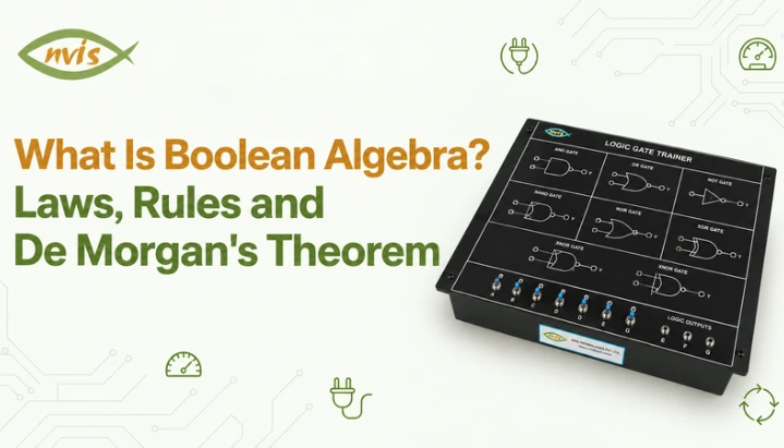
Dedicated trainer kits, such as the Nvis 6553 De Morgan’s Theorem Trainer, are designed specifically for this type of laboratory exercise. The kit provides separate sections for demonstrating the two De Morgan’s theorems, allowing students to wire and test each circuit independently. It can also help students understand universal gate concepts through practical circuit connections. This kind of hands-on verification is what turns an algebraic identity into a working understanding of why NAND and NOR gates are chosen for real IC families. A broader look at what a digital electronics lab needs to run this and related experiments is covered in Nvis Tech’s guide to what a digital electronics laboratory should include.
Boolean Algebra Laws vs. De Morgan’s Theorem: A Quick Comparison
| Aspect | Basic Boolean Algebra Laws | De Morgan’s Theorem |
| Number of rules | Nine standard laws (identity, null, idempotent, complement, involution, commutative, associative, distributive, absorption) | Two related rules |
| Primary use | Simplifying expressions by combining or eliminating terms | Converting between AND and OR operations across a complement |
| Circuit level meaning | Reduces gate count for a given logic family | Enables implementation using only NAND or only NOR gates |
| Proof method | Perfect induction (truth table) for each law individually | Perfect induction, or algebraic proof via uniqueness of complement |
| Typical exam use | Expression simplification, minimal SOP/POS forms | Removing nested complements, universal gate conversion problems |
Where Does Boolean Algebra Fit in GATE, SSC JE, and RRB JE Preparation?
Boolean algebra and De Morgan’s theorems are part of digital logic, which is covered in the GATE syllabi for relevant engineering disciplines, including Electronics and Communication Engineering (ECE), Electrical Engineering (EE), and Instrumentation Engineering (IN). Questions may involve Boolean expression simplification, logic gates, and combinational circuit design. These topics can become relatively straightforward exam questions once the underlying laws and De Morgan’s theorem are well understood, since they follow fixed, mechanical steps rather than requiring deeper derivation needed for some other digital logic topics.
Depending on the specific technical discipline and examination syllabus, SSC JE and RRB JE candidates may encounter Boolean algebra and logic-gate fundamentals in their technical preparation, since these exams weigh foundational concepts heavily. Boolean simplification and logic-gate concepts can also be relevant in technical interviews for electronics, electrical, and instrumentation engineering roles, where candidates may be asked to simplify Boolean expressions or explain logic-gate equivalence.
Conclusion
Boolean algebra provides the mathematical foundation for digital electronics. Its nine core laws, including identity, null, idempotent, complement, involution, commutative, associative, distributive, and absorption, form an essential toolkit for simplifying Boolean expressions. De Morgan’s theorem extends that toolkit with a specific, high value rule: it converts between AND and OR operations across a complement, and it is the reason a single gate type, NAND or NOR, can build any digital circuit on its own. Between algebraic proof and truth table proof covered here, and worked simplification example, a student should now be able to state and prove De Morgan’s theorem independently and apply it to reduce a nested Boolean expression. For GATE, SSC JE, and RRB JE preparation, treat these laws as mechanical tools to practice until they are automatic, since practicing these laws can help you solve many Boolean simplification and logic-gate questions more efficiently. Work through a few practice simplification problems using only laws covered here, then verify results by building an equivalent circuit on a trainer kit or simulator to see if the same identity holds true on real hardware.
FAQs
What is the difference between Boolean algebra and ordinary algebra?
In basic Boolean algebra, variables take only two possible values, 0 and 1. The fundamental operations are AND, OR, and NOT, which are used to construct and simplify logical expressions. Unlike ordinary arithmetic, subtraction and division are not standard operations in Boolean algebra. Ordinary algebra works over real numbers with a continuous range of values and includes addition, subtraction, multiplication, and division. Some identities, such as OR distributing over AND, hold in Boolean algebra but have no equivalent in ordinary algebra.
How many laws are there in Boolean algebra?
Nine laws cover core simplification toolkit: identity, null (annulment), idempotent, complement, involution, commutative, associative, distributive, and absorption. De Morgan’s theorem is often taught alongside these as a tenth, closely related identity, though it is technically a separate theorem rather than one of nine basic laws.
Why are NAND and NOR called universal gates?
NAND and NOR are each capable of implementing NOT, AND, and OR on their own, and therefore any Boolean function whatsoever, which is a direct consequence of De Morgan’s theorem. This is why NAND and NOR gates are important building blocks in digital logic and why NAND and NOR are widely used as universal building blocks in digital logic. The 7400-series families include a wide range of logic functions, including NAND, NOR, inverter, AND, OR, and other devices.
Can De Morgan's theorem be applied to more than two variables?
Yes. Both theorems extend to any number of variables using the same pattern: the complement bar over a group of ANDed or ORed variables breaks into individual complement bars over each variable, and the operator between them flips from AND to OR or from OR to AND. For example, (A + B + C)′ = A′B′C′.
Is Boolean algebra asked about in GATE, SSC JE, and RRB JE exams?
Boolean algebra and De Morgan’s theorem are a consistently tested part of the digital logic section in GATE ECE, EE, and IN papers, usually as simplification or gate equivalence questions. SSC JE and RRB JE technical papers for electronics and electrical trades also test these fundamentals directly, and PSU technical interviews frequently include a live expression simplification question.
What is the quickest way to check if a Boolean simplification is correct?
Build a truth table for both original expression and simplified expression, and confirm that the output column matches for every combination of input values. This is the same perfect induction method used to prove basic laws and De Morgan’s theorem, and it works for any Boolean identity regardless of how many variables it involves.