TL;DR
- The article is aimed at engineering and diploma students, as well as GATE, SSC JE, and RRB JE candidates who want an easy-to-understand explanation of logic gates and digital circuits.
- A logic gate is an electronic circuit that implements a Boolean function by converting one or more binary inputs into a single binary output according to predefined logic rules.
- Seven common types of logic gates AND, OR, NOT, NAND, NOR, XOR, and XNOR have their own symbols, truth tables, and Boolean expressions.
- Both NAND and NOR are known as universal gates because each can be used to construct the other basic logic gates and, therefore, any Boolean function. This concept is commonly tested in digital electronics exams.
- Logic gates are essential building blocks of digital circuits, including calculator arithmetic units, processors, and satellite onboard computers. They are used to build both combinational and sequential circuits.
A logic gate is a basic building block of digital electronics. It accepts one or more binary inputs and produces a binary output according to a defined logical rule. In practical circuits, gates are implemented using electronic components such as transistors and are combined to build larger digital systems.
Logic gates are important in electronic devices for much more than just textbook concepts. Digital circuit design is an important part for GATE ECE, EE and IN exams while also appearing on SSC JE and RRB JE technical papers too. VLSI engineers and embedded systems developers use digital logic concepts when designing circuits, writing RTL code, and working with programmable or integrated digital systems.This article explains logic gate definitions, symbols, truth tables, and Boolean expressions. It also explains why NAND and NOR are called universal gates, with examples relevant to digital electronics exams.
Also Read,
What Do You Need to Know Before Logic Gates?
Logic gates rest on two ideas: binary representation and Boolean algebra.Digital circuits use two logic states, usually represented as LOW and HIGH. These states correspond to voltage ranges rather than two exact voltage values. For standard TTL inputs, voltages up to about 0.8 V are generally recognized as LOW, while voltages above about 2 V are recognized as HIGH. CMOS logic levels depend on the specific device and its supply voltage. All signals within an electronic device are represented by numbers, characters, and command codes which can be expressed through sequences of bits.The Boolean algebra was invented by George Boole as an algebraic system for describing combinations of two-valued variables. Boolean algebra defines three basic operations: AND, represented by logical multiplication; OR, represented by logical addition; and NOT, which represents complementation. Logic gates are just an implementation by means of electronics for some type of Boolean operation (or combinations thereof). After understanding those concepts clearly, it would be easy to understand how each gate works by following their truth tables properly.
What Is a Logic Gate?
A logic gate is a digital circuit with one or more binary inputs and exactly one binary output, where output depends entirely on the current combination of inputs according to a defined logic function. Internally, gates are built from transistors (in modern ICs, almost always MOSFETs in CMOS technology), but at design level, engineers work with the gate as an abstract logic block rather than its internal transistor circuit.Each gate is described using three equivalent representations that appear constantly in coursework and exams: logic symbol, used in circuit diagrams; truth table, which lists output for every possible input combination; and Boolean expression, which states the same relationship algebraically. Being able to move between these three representations is an important skill in digital electronics.
Types of Logic Gates With Symbols, Truth Tables, and Boolean Expressions
The seven commonly discussed logic gates are AND, OR, NOT, NAND, NOR, XOR, and XNOR. AND, OR, and NOT are the basic gates, while NAND and NOR are universal gates. XOR and XNOR are commonly used in arithmetic, comparison, and other digital logic applications.
AND Gate
AND gate produces a HIGH output only when all of its inputs are HIGH. Its Boolean expression is Y = A·B for a two input gate, and it is represented in circuit diagrams by a D shaped symbol with a flat input side. A common TTL implementation is the 7408, which contains four 2-input AND gates.
AND gate behaves the way word “and” does in everyday language: a condition is true only when every requirement is met together. A safety interlock circuit that must confirm both a door is closed and a machine guard is in place before allowing a motor to start is a direct real world instance of AND logic.
OR Gate
OR gate produces a HIGH output when at least one input is HIGH. Its Boolean expression is Y = A + B, and its symbol has a curved input side that tapers to a point at output. A common TTL part is IC 7432, a quad 2 input OR gate.
OR logic matches situations where any one of several conditions is sufficient to trigger an action, such as a fire alarm circuit that should sound if a smoke sensor or a heat sensor detects a hazard, since either input alone should activate the alarm.
NOT Gate
A NOT gate, also called an inverter, is only a gate with a single input. It inverts its input: a 0 becomes 1, and a 1 becomes 0. Its Boolean expression is written as Y = A’ or Y = Ā, and its symbol is a triangle followed by a small circle (bubble) at output, where bubble specifically denotes inversion. IC 7404 is a hex inverter, packing six independent NOT gates in one chip.
The inversion bubble is worth remembering carefully, because the same bubble symbol appears on the output of NAND and NOR gates, and confusing where it is placed is one of most common mistakes in exam diagrams.
NAND Gate
A NAND gate can be considered as an AND gate followed by another NOT gate. It produces a LOW output only when all of its inputs are HIGH; otherwise, the output is HIGH. Its Boolean expression is Y = (A·B)’. The apostrophe indicates that the AND operation is inverted. The 7400 is a standard quad 2-input NAND gate. NAND is a universal gate, meaning NAND gates can be combined to implement other basic logic functions.
NOR Gate
NOR gate (NOT OR) is an OR gate followed by a NOT gate. Its output is HIGH only when all inputs are LOW. Boolean expression is Y = (A+B)’, and the symbol is an OR gate shape with an inversion bubble at output. IC 7402 is a standard quad 2 input NOR gate.
Why Are NAND and NOR Called Universal Gates?
NAND and NOR are called universal gates because either type can be used alone to implement NOT, AND, OR, and, therefore, any Boolean function. ITheir universality means that a complete logic function can be constructed using only NAND gates or only NOR gates, which is an important concept in digital logic design.For example, a NOT gate can be implemented using a NAND gate by connecting both NAND inputs to the same signal, connect both inputs of the NAND gate to the same signal:Y = (A·A)’ = A’By connecting both inputs of a NAND gate to the same signal, the NAND gate acts as a NOT gate. NAND gates can then be combined to implement AND and OR operations using Boolean algebra and De Morgan’s laws. Using De Morgan’s laws, NAND gates can also be combined to implement OR functions. For example, an OR gate can be built as:A + B = (A’·B’)’The same basic approach can be used to implement NOT, OR, and AND using only NOR gates, with De Morgan’s laws providing the required transformations.XOR GateXOR (Exclusive OR) gate produces a HIGH output only when its inputs differ from each other. Its Boolean expression is Y = A ⊕ B = AB’ + A’B, and its symbol resembles OR gate but with an extra curved line at input side. IC 7486 is a standard quad 2 input XOR gate.
XOR is an important building block in binary addition. In a half adder, the Sum output is produced using XOR, while full adders also use XOR as part of their sum-generation logic.
XNOR Gate
XNOR (Exclusive NOR) gate is a complement of XOR: it produces a HIGH output only when its inputs match. Its Boolean expression is Y = (A⊕B)’ = AB + A’B’, and its symbol is XOR symbol with an added inversion bubble at output. IC 74266 is a commonly used quad 2 input XNOR gate.
Because it outputs HIGH exactly when inputs agree, XNOR is the natural building block for equality comparator circuits, which check whether two binary numbers are identical bit by bit.
Worked Example: Minimizing a Boolean Function and Realizing It With Gates
Digital-logic problems may require students to simplify a Boolean function and then implement the resulting expression using logic gates. The following example demonstrates that process and then drawing its gate level circuit, a two step process worth walking through with an actual problem.Consider a three variable function F(A, B, C) defined by the truth table below, where F = 1 for minterms 0, 2, 4, 5, and 6.
| A | B | C | F |
| 0 | 0 | 0 | 1 |
| 0 | 0 | 1 | 0 |
| 0 | 1 | 0 | 1 |
| 0 | 1 | 1 | 0 |
| 1 | 0 | 0 | 1 |
| 1 | 0 | 1 | 1 |
| 1 | 1 | 0 | 1 |
| 1 | 1 | 1 | 0 |
Plotting this on a 3 variable Karnaugh map shows two groupable patterns. First, the entire C = 0 column is filled with 1s across all four AB combinations, which reduces to single term C’. Second, AB = 10 rows (A = 1, B = 0) is entirely 1 across both values of C, which reduces to the term AB’. Together, these two groups cover every 1 in the table with no overlap left uncovered.minimized Boolean expression is therefore:F = C’ + AB’To realize this with gates: pass C through a NOT gate to get C’, pass B through a separate NOT gate to get B’, feed A and B’ into a 2 input AND gate to get AB’, and finally feed C’ and AB’ into a 2 input OR gate to produce F. complete circuit uses four gates in total: two NOT gates, one AND gate, and one OR gate. This illustrates the type of Boolean minimization and combinational-circuit implementation problem that can be encountered in digital-electronics examinations.
Where Are Logic Gates Used?
Logic gates appear anywhere a decision needs to be made from binary conditions. Arithmetic logic units inside processors use combinations of XOR, AND, and OR gates to perform addition and subtraction.
Address decoders in memory systems use AND and NAND gates to select a specific memory location from a binary address. Digital locks and security systems combine gates to check multiple input conditions before granting access. Traffic light controllers, elevator control panels, and automatic street light circuits that switch on based on a light sensor all rely on gate level logic underneath their control software. Even a simple calculator performs every arithmetic operation through layers of logic gates built into its integrated circuit.
How Are Logic Gates Built: TTL vs CMOS?
Logic gates have historically been implemented using different logic families, two important examples being TTL (Transistor-Transistor Logic) and CMOS (Complementary Metal-Oxide-Semiconductor).TTL gates, found in 74xx series of ICs such as 7400 and 7408, are built using bipolar junction transistors and were the dominant logic family through 1970s and 1980s. CMOS gates are found in families such as the 40xx and 74HCxx series. TTL families include the original 74xx and 74LSxx series. CMOS logic families became dominant in modern IC design largely because of their very low static power consumption and high integration capability. CMOS logic has very low static power consumption compared with traditional TTL, which makes it well suited to highly integrated modern digital systems. Modern processors and memory devices are based on CMOS technologies rather than traditional TTL logic families.
| Parameter | TTL | CMOS |
| Base technology | Bipolar junction transistors | MOSFETs (NMOS + PMOS pairs) |
| Power consumption | Higher static power draw | Very low static power draw |
| Supply voltage | Typically 5 V | Wide range, from below 2 V to 15 V depending on family |
| Noise margin | Moderate | Generally higher |
| Common IC series | 74xx, 74LSxx | 40xx, 74HCxx |
Applications of Logic Gates in Industry
Digital electronics play an important role in defence and space systems. Bharat Electronics Limited (BEL) develops defence and communication electronics, while ISRO uses digital electronics in spacecraft, launch vehicles, and associated onboard systems.India’s semiconductor initiatives have increased attention on domestic semiconductor design and manufacturing, making digital logic fundamentals relevant to careers in areas such as chip design and verification, since gate level thinking underlies every stage of chip design from RTL coding to physical layout.
Why Logic Gates Matter for GATE, SSC JE, and RRB JE?
Digital logic, including logic gates, Boolean minimization, and combinational circuits, is an explicitly listed topic in the Digital Circuits section of GATE ECE syllabus, alongside sequential circuits, data converters, and computer organization. The same core concepts are tested in GATE EE and GATE IN papers, Digital circuits is part of the relevant GATE syllabi, and questions can involve Boolean algebra, logic gates, combinational circuits, and sequential circuits.For SSC JE and RRB JE Electronics papers, logic gates form part of the digital electronics section and are tested through direct questions on truth tables, gate identification from a given symbol, Boolean simplification, and universal gate implementation. Question formats and difficulty vary by examination and year, so candidates should prepare both direct concept questions and circuit-based problems, which makes a solid grasp of each gate’s truth table and symbol especially valuable for scoring quickly.It is worth noting that the GATE syllabus has changed over time, so candidates should always refer to the current official syllabus when preparing. This does not affect logic gates or digital logic in general, which remain a core, examined topic. Candidates should refer to the latest examination syllabus and recruitment notification for the exact topics covered.
Career and Recruitment Context
A solid foundation in logic gates and digital logic design opens several engineering career paths in India. Digital design engineers and VLSI/ASIC design engineers work directly with gate level and RTL design as part of chip development teams. Embedded systems engineers use digital logic concepts when interfacing microcontrollers with sensors and peripheral circuits. Recruitment routes vary across PSUs, roles, and recruitment cycles. Some technical positions use GATE scores as part of the selection process, while others use separate recruitment examinations or selection procedures, while SSC JE and RRB JE recruit junior engineers directly through their own technical examinations, both of which test digital logic fundamentals.For SSC JE and RRB JE candidates, the relevance of digital logic depends on the specific post and applicable syllabus. Candidates should check the current examination notification for the subjects and technical topics applicable to their post.Logic Gates at a Glance
| Gate | Boolean Expression | Output is HIGH when | Common IC |
| AND | Y = A·B | All inputs are HIGH | 7408 |
| OR | Y = A+B | Any input is HIGH | 7432 |
| NOT | Y = A’ | Input is LOW | 7404 |
| NAND | Y = (A·B)’ | Any input is LOW | 7400 |
| NOR | Y = (A+B)’ | All inputs are LOW | 7402 |
| XOR | Y = A⊕B | Inputs differ | 7486 |
| XNOR | Y = (A⊕B)’ | Inputs match | 74266 |
Conclusion
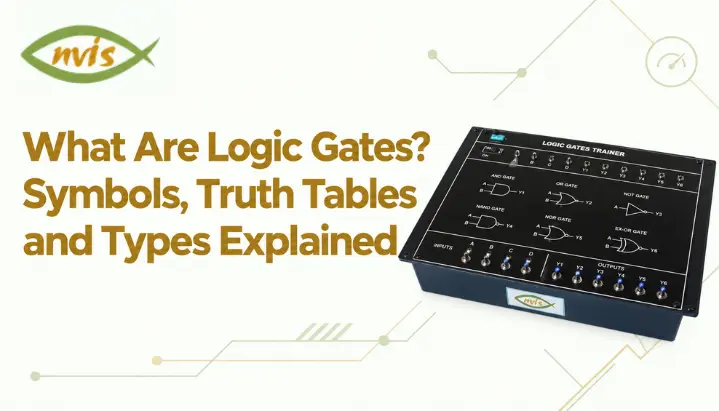
Logic gates convert binary inputs into a single binary output based on a fixed Boolean rule, and every digital circuit, from a calculator to a satellite’s onboard computer, is built by combining them. Seven standard gates, AND, OR, NOT, NAND, NOR, XOR, and XNOR, each carry their own symbol, truth table, and Boolean expression, and NAND and NOR earn the label “universal” because either one alone can reproduce every other gate. Digital logic is an important area of study for relevant GATE, SSC JE, and RRB JE technical syllabi, and the same fundamentals carry directly into PSU technical interviews and engineering roles in VLSI and embedded systems design.Reading a truth table correctly and moving between symbol, truth table, and Boolean expression without hesitation is a skill built through hands-on practice rather than memorization alone. Students who want to move past textbook explanations and build, test, and observe real logic gate circuits can start with the
Logic Gates Experimentation Kit from NVIS Technologies, designed specifically for hands-on digital electronics learning.
FAQs