





TL;DR
- This blog is for engineering and diploma students, GATE ECE/EE aspirants, and RRB JE Electronics candidates who need a clear, exam ready understanding of shift registers and how each type moves data.
- A shift register is a chain of flip flops that stores and moves binary data one bit position per clock pulse, and its behavior is fixed by how data enters and leaves the chain.
- The common SISO, SIPO, PISO and PIPO classifications describe how data enters and leaves a register: serially, in parallel, or a combination of both.
- A universal shift register such as the 74194/74HC194 combines serial shifting in both directions, parallel loading, and hold operation on one chip using mode-select inputs, which is why it shows up repeatedly in GATE and RRB JE digital electronics questions.
- Shift registers are not a theoretical topic. They run inside SPI communication, LED matrix drivers, UART transmitters, and I/O expander chips used in real embedded designs.
Also Read,
- Arduino for Embedded Systems Learning: Setting Up Your First Lab Project
- IoT Microcontroller Projects for Engineering Students: From Sensor to Cloud
- ARM Cortex M Microcontrollers Explained: Architecture for Embedded Engineering Students
What You Need to Know Before Shift Registers
A shift register is built entirely from flip flops, so understanding it starts with understanding what a flip flop does. A flip flop is a one bit memory element that captures value present at its input on a clock edge and holds that value steady until the next active edge arrives. D flip flop is type almost universally used inside shift registers, because it copies whatever logic level is on its D input to its Q output moment clock transitions from low to high (or high to low, depending on design). A register, in general, is simply a group of flip flops that share a common clock line and store multiple bits together, the same way a byte in memory stores eight bits as one unit. A shift register is a special case of a register where flip flops are wired in series rather than in parallel: Q output of first flip flop connects to D input of second, second’s Q connects to third’s D, and so on down the chain. Because every flip flop in the chain shares the same clock, all of them update simultaneously on each clock edge, and the effect is that the entire bit pattern appears to slide one position to right (or left) every clock cycle.How Data Moves Through a Shift Register
Consider a 4 bit shift register made of flip flops FF0, FF1, FF2 and FF3, connected so FF0’s output feeds FF1’s input, FF1’s feeds FF2’s, and FF2’s feeds FF3’s. A new bit is applied to FF0’s input just before each clock edge. When the clock ticks, FF0 captures a new bit, FF1 captures what FF0 held a moment ago, FF2 captures what FF1 held, and FF3 captures what FF2 held. bit that was sitting in FF3 is pushed out of the register entirely. This is a mechanical action every shift register performs, regardless of type. What changes between SISO, SIPO, PISO, PIPO and universal shift registers is only the answer to two questions: how does data get into the register, and how is data read back out. Data can enter or exit either serially, meaning one bit is presented per clock pulse through a single line, or in parallel, meaning all bits are presented or read simultaneously through separate lines connected to every flip flop at once.Serial In Serial Out (SISO)
A SISO shift register accepts one bit at a time on its serial input and, after bits have propagated through the full chain, releases them one at a time from the final flip flop’s output. No parallel access to intermediate stages is provided. An n-bit SISO register requires n clock edges for an input bit to propagate through all n stages, making it useful as a digital delay element. For a 4-bit register, the exact timing convention used to describe the delay should be stated when calculating latency.Serial In Parallel Out (SIPO)
A SIPO shift register also accepts data serially, one bit per clock pulse on a single input line, but every flip flop’s Q output is brought out to its own pin. After n clock pulses have loaded n bits into an n bit register, all n bits are available simultaneously on parallel outputs. This is the exact configuration used to convert a serial bitstream, such as data arriving over a single wire from a sensor or a communication bus, into a parallel word a microcontroller or logic circuit can read in one step. widely used 74HC164 and 74HC595 families are built around this principle, with 74HC595 adding an output latch so parallel outputs update only when commanded, keeping the shifting process invisible to whatever is reading outputs.Parallel In Serial Out (PISO)
A PISO shift register does the reverse of SIPO. All n bits are loaded into register simultaneously through n separate parallel input lines, typically during a load pulse, and are then shifted out one bit at a time through a single serial output line over following n clock pulses. Because each flip flop needs to select between two possible next inputs, either parallel data bit during load or previous stage’s output during shifting, PISO registers use a multiplexer in front of every flip flop, controlled by a shared load/shift control line. 74HC165 is a common PISO IC, and this configuration is a standard way to read several parallel switch or sensor inputs using only one data line back to a controller, This approach allows a controller to read multiple parallel inputs using a small number of interface lines.Parallel In Parallel Out (PIPO)
PIPO is often included alongside SISO, SIPO, and PISO when classifying register data-transfer modes. However, a PIPO register does not perform serial shifting; it loads and reads all bits in parallel and is better viewed as a parallel register or storage register. It loads all n bits in parallel and makes them available on parallel outputs, so it behaves more like a parallel storage or buffer register. Strictly speaking, a PIPO configuration does not shift data through a chain the way other three types do; it behaves as a straightforward parallel buffer or temporary storage register, and it is included in the shift register family because the same flip flop chain hardware can be wired to support this mode alongside others.Universal Shift Register
A universal shift register is a single IC that supports serial and parallel data operations, including shift-right, shift-left, hold, and parallel-load modes, with shifting in both directions, and switches between them using dedicated mode select inputs rather than requiring separate circuits for each function. 74194 (and its faster CMOS version, 74HC194) is standard textbook and lab example, and its internal structure illustrates exactly why a universal shift register needs more than just a chain of flip flops. Each flip-flop stage in the 74194 is preceded by selection logic that chooses the appropriate next value from the parallel input, the neighboring stage, the appropriate serial input, or its current state. The S1 and S0 mode-select inputs determine whether the register holds its current value, shifts right, shifts left, or loads data in parallel. Internally, selection logic before each flip-flop chooses the appropriate next input for the selected mode. The S1 and S0 inputs determine whether the register holds, shifts left, shifts right, or parallel-loads, or its own current output (to hold its value unchanged). Two mode select inputs, commonly labelled S1 and S0, control which of these four choices every multiplexer in chip makes simultaneously, so same hardware behaves as a hold register, a right shifting SIPO/SISO register, a left shifting register, or a PIPO parallel load register depending on what logic levels are placed on S1 and S0.| S1 | S0 | Operating mode |
| 0 | 0 | Hold (no change, data retained) |
| 0 | 1 | Shift right, serial data entered through DSR |
| 1 | 0 | Shift left, serial data entered through DSL |
| 1 | 1 | Parallel load, data D0 to D3 loaded into Q0 to Q3 |
Worked Example Tracing Data Through a 4 Bit Shift Register
A short numerical trace makes shifting action concrete and mirrors the style of question asked in GATE and RRB JE digital electronics papers. Consider a 4 bit register with outputs Q0 Q1 Q2 Q3, initially holding 1 0 1 0, configured to shift right on every clock pulse (data advances from Q0 toward Q3) with a serial input DSR that supplies 0, 1, 1, 0 on four successive clock pulses. On each pulse, a new serial bit enters at Q0, every stored bit moves one place toward Q3, and the bit that was in Q3 is shifted out and lost. Before any clock pulse: Q0 Q1 Q2 Q3 = 1 0 1 0. After clock pulse 1 (DSR = 0): bit in Q3 (which was 0) shifts out, every remaining bit moves one place toward Q3, and new serial bit 0 enters at Q0. register now reads 0 1 0 1. After clock pulse 2 (DSR = 1): bit in Q3 (1) shifts out, register content shifts right, and 1 enters at Q0. register now reads 1 0 1 0. After clock pulse 3 (DSR = 1): following the same rule, register becomes 1 1 0 1. After clock pulse 4 (DSR = 0): register becomes 0 1 1 0. This trace shows two things that exam questions routinely test. First, bit shifted out of Q3 is genuinely lost unless it is captured externally, since a simple shift register has no feedback path of its own. Second, after exactly n = 4 clock pulses in a 4 bit register, every original bit has been shifted completely out, which is basis for calculating how many clock pulses a SISO or PISO register needs to fully load or unload a known bit pattern, a calculation that appears directly in past GATE ECE and GATE EE sequential circuits questions.Applications of Shift Registers in Real Circuits
Shift registers are not confined to textbook diagrams. SIPO registers such as 74HC595 devices are commonly used to expand digital outputs for applications such as seven-segment displays, LED indicators, and some LED-matrix designs, allowing a microcontroller to send data serially while controlling multiple parallel outputs because parallel outputs can drive many LEDs while microcontroller only has to send data serially. PISO registers such as the 74HC165 can read a bank of parallel switches or sensor lines and send their states to a controller over a serial connection. Similar serial interfaces are also used in some input-expansion designs. The Serial Peripheral Interface (SPI) protocol used throughout embedded systems is itself built on shift register behavior: at hardware level, both master and slave devices contain internal shift registers, and each clock pulse simultaneously shifts a bit out of one device and into another. A UART transmitter typically uses shift-register-based serialisation to convert parallel transmit data into a serial bitstream, along with timing and framing logic for start and stop bits on the transmit line, A UART receiver uses serial sampling, timing, framing, and shift-register-based data collection to reassemble incoming bits into parallel data. Shift registers also form the basis of ring counters and Johnson counters, sequential circuits built by feeding a shift register’s output back to its own input, which are used for generating timing sequences and simple state machines in control circuits.Learning Shift Registers Hands On
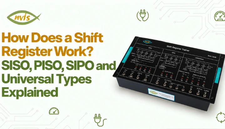
Reading a function table explains what a universal shift register should do, but watching mode select logic switch between hold, shift left, shift right and parallel load behavior on real hardware is what makes the concept stick for lab exams and viva questions. A dedicated trainer board that lets a student wire and test all four basic shift register types on one platform, such as Shift Registers Trainer, removes guesswork of breadboard wiring errors and lets LED indicators show bit pattern moving through register on every clock pulse, which is a faster way to internalize shifting action than working through timing diagrams alone.Shift Registers in GATE, RRB JE and Technical Exams
Shift registers are explicitly listed under Digital Electronics in the GATE 2026 Instrumentation Engineering syllabus. For GATE EC, sequential circuits are included in the syllabus, but the EC syllabus wording should be checked before stating that “shift registers” are explicitly named. They are also relevant to the sequential-logic portion of GATE EE’s digital electronics coverage, and Shift-register concepts have been tested in GATE digital/sequential-circuit questions, including questions involving timing, shifting and bit patterns including numerical questions that ask how many clock pulses are needed for a given register to return to its original state. This is distinct from older GATE ECE syllabus coverage of microprocessors. In the current GATE 2026 EC syllabus, shift registers remain explicitly listed under Sequential Circuits, while Computer Organization covers topics such as machine instructions, ALU, datapaths, and control units. For RRB JE, Electronics and Communication and Electronics and Telecommunication streams list Digital Electronics explicitly as a technical ability topic in CBT 2 syllabus, and Digital Electronics is included in the technical syllabus, covering combinational and sequential logic circuits, counters, memories and related topics; shift registers can be studied as part of sequential-logic preparation. SSC JE coverage depends on the engineering discipline and the applicable recruitment notification. Candidates should check the current official syllabus rather than assuming that shift registers are a separately listed topic, so candidates preparing specifically for SSC JE Electrical should weight their preparation time accordingly, while SSC JE Electronics candidates and Shift-register fundamentals can also be relevant in technical interviews for electronics, embedded-systems and digital-design roles.Where Shift Register Knowledge Applies on Job
Shift registers sit inside digital design, embedded systems and VLSI roles far more often than most students expect, since any system that talks over SPI, drives an LED matrix, or expands GPIO pins is very likely using shift register logic internally. Sequential digital circuits can be relevant preparation topics for electronics-focused technical interviews, particularly for roles involving digital systems, embedded systems, or electronics design for junior engineer and trainee roles, and a solid grasp of how SISO, SIPO, PISO, PIPO and universal shift registers behave is exactly kind of fundamental that separates a rehearsed answer from a genuine understanding during those interviews.Comparing Shift Register Types
| Type | Data input | Data output | Clock pulses to load/read n bits | Typical IC | Common use |
| SISO | Serial | Serial | n | 74HC164 (wired serial out) | Timing delay element |
| SIPO | Serial | Parallel | n | 74HC164, 74HC595 | Serial to parallel conversion, LED/display drivers |
| PISO | Parallel | Serial | n | 74HC165 | Parallel to serial conversion, input expanders |
| PIPO | Parallel | Parallel | 1 | Generic parallel registers | Temporary data storage/buffering |
| Universal | Serial or parallel | Serial or parallel | Depends on mode selected | 74194 / 74HC194 | Bidirectional shifting, parallel loading, and flexible data movement; shifting can also be used in some binary arithmetic operations. |
Conclusion
A shift register is fundamentally a chain of flip flops that moves stored bits one position on every clock pulse, and the basic SISO, SIPO, PISO and PIPO classifications describe how data enters and leaves the register, while universal shift registers add selectable operating modes such as shifting, holding, and parallel loading SISO registers use serial input and serial output and can be used for serial data delay, while PISO registers accept parallel data and shift it out serially for parallel-to-serial conversion, SIPO handles serial to parallel conversion for driving displays and reading serial data streams, PIPO acts as a simple parallel buffer, and universal shift register, exemplified by 74194/74HC194, combines all these behaviors using mode select inputs so a single chip can be reconfigured for whichever function a design needs. These circuits are not an isolated exam topic; they run inside SPI communication, UART data framing, LED matrix drivers and GPIO expanders in real embedded hardware, which is why concept keeps showing up from GATE sequential circuits questions through to PSU technical interviews. Building and testing all four types on a lab trainer, then working through a few bit pattern tracing problems by hand, is the most direct way to move from recognizing a function table to being able to design with it.Frequently Asked Questions
What is the main difference between a shift register and a normal register?
A normal parallel register loads and reads all its bits simultaneously and does not move data between its flip flops. A shift register is specifically wired so that data moves one flip flop position along a chain on every clock pulse, which is what allows it to convert between serial and parallel data formats.
Why does a PISO shift register need multiplexers but a SIPO register does not?
A PISO register must choose, on every clock edge, between loading a new parallel bit during load phase and shifting in previous stage’s output during shift phase, and a multiplexer in front of each flip flop makes that selection. A basic SIPO register only ever shifts data in from serial input, so no such selection is needed at each stage.
How many clock pulses does an 8 bit SIPO shift register need to output valid parallel data?
Exactly 8 clock pulses, since each pulse loads one new serial bit into the first flip flop and shifts existing bits one position further down the 8 bit chain. parallel outputs only reflect a complete 8 bit word once all 8 bits have been clocked in.
What does 74194 do differently from a basic shift register IC?
74194 is a universal shift register: its two mode select inputs (S1, S0) let it operate as a hold register, a right shift register, a left shift register, or a parallel load register, all on the same chip, instead of being hardwired to only one of those behaviors.
Are shift registers still relevant for GATE preparation after microprocessors were removed from GATE ECE syllabus?
Yes. Shift registers are explicitly included under Sequential Circuits in the GATE 2026 ECE syllabus. They are also relevant to sequential-logic coverage in other GATE papers where digital electronics is part of the syllabus, which is separate from microprocessor and computer organization topics that GATE ECE dropped in 2022. Sequential circuit questions involving shift registers continue to appear in GATE papers.
Where are shift registers used outside of academic circuits?
Shift registers operate inside SPI communication hardware, UART transmitters and receivers, LED matrix and seven segment display drivers such as 74HC595, and parallel-input shift registers such as the 74HC165, which can be used to expand the number of digital inputs available to a microcontroller, making them a routine part of embedded systems and digital hardware design rather than a purely theoretical topic.